SCES586D July 2004 – June 2015 SN74LVC1G123
PRODUCTION DATA.
- 1 Features
- 2 Applications
- 3 Description
- 4 Revision History
- 5 Pin Configuration and Functions
-
6 Specifications
- 6.1 Absolute Maximum Ratings
- 6.2 ESD Ratings
- 6.3 Recommended Operating Conditions
- 6.4 Thermal Information
- 6.5 Electrical Characteristics
- 6.6 Timing Requirements
- 6.7 Switching Characteristics, CL = 15 pF, -40°C to 85°C
- 6.8 Switching Characteristics, CL = 50 pF, -40°C to 85°C
- 6.9 Switching Characteristics, CL = 50 pF, -40°C to 125°C
- 6.10 Operating Characteristics
- 6.11 Typical Characteristics
- 7 Parameter Measurement Information
- 8 Detailed Description
- 9 Application and Implementation
- 10Power Supply Recommendations
- 11Layout
- 12Device and Documentation Support
- 13Mechanical, Packaging, and Orderable Information
Package Options
Mechanical Data (Package|Pins)
Thermal pad, mechanical data (Package|Pins)
Orderable Information
8 Detailed Description
8.1 Overview
The SN74LVC1G123 device is a single retriggerable monostable multivibrator designed for 1.65-V to 5.5-V VCC operation.
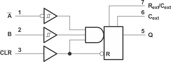
This monostable multivibrator features output pulse-duration control by three methods. In the first method, the A input is low, and the B input goes high. In the second method, the B input is high, and the A input goes low. In the third method, the A input is low, the B input is high, and the clear (CLR) input goes high.
The output pulse duration is programmed by selecting external resistance and capacitance values. The external timing capacitor must be connected between Cext and Rext/Cext (positive) and an external resistor connected between Rext/Cext and VCC. To obtain variable pulse durations, connect an external variable resistance between Rext/Cext and VCC. The output pulse duration also can be reduced by taking CLR low.
Pulse triggering occurs at a particular voltage level and is not directly related to the transition time of the input pulse. The A and B inputs have Schmitt triggers with sufficient hysteresis to handle slow input transition rates with jitter-free triggering at the outputs.
Once triggered, the basic pulse duration can be extended by retriggering the gated low-level-active (A) or high-level-active (B) input. Pulse duration can be reduced by taking CLR low. CLR can be used to override A or B inputs. The input/output timing diagram illustrates pulse control by retriggering the inputs and early clearing.
The SN74LVC1G123 device is fully specified for partial-power-down applications using Ioff. The Ioff circuitry disables the outputs, preventing damaging current backflow through the device when it is powered down.
NanoFree™ package technology is a major breakthrough in IC packaging concepts, using the die as the package.
8.2 Functional Block Diagram

8.3 Feature Description
This part is available in the Texas Instruments NanoFree™ package. It supports 5-V VCC operation and accepts inputs up to 5.5 V. The max tpd is 8 ns at 3.3 V. It supports mixed-mode voltage operation on all ports.
Down translation can be achieved to VCC from up to 5.5 V.
Schmitt-trigger circuitry on A and B inputs allows for slow input transition rates. The device can be edge triggered from active-high or active-low gated logic inputs. It can support up to 100% duty cycle from retriggering.
Clear can be used to terminate the output pulse early.
Glitch-free power-up reset is on all outputs.
Ioff supports live insertion, partial-power-down mode, and back-drive protection.
Latch-up performance exceeds 100 mA per JESD 78, Class II.
8.4 Device Functional Modes
Table 1 lists the functional modes for the SN74LVC1G123.
