SGES002E April 2003 – August 2020 SN74LVC1G125-Q1
PRODUCTION DATA
- 1 Features
- 2 Applications
- 3 Description
- 4 Revision History
- 5 Pin Configuration and Functions
- 6 Specifications
- 7 Parameter Measurement Information
- 8 Detailed Description
- 9 Application and Implementation
- 10Power Supply Recommendations
- 11Layout
- 12Device and Documentation Support
- 13Mechanical, Packaging, and Orderable Information
Package Options
Refer to the PDF data sheet for device specific package drawings
Mechanical Data (Package|Pins)
- DBV|5
- DCK|5
- DRY|6
Thermal pad, mechanical data (Package|Pins)
- DRY|6
Orderable Information
3 Description
This bus buffer gate is designed for 1.65-V to 5.5-V VCC operation.
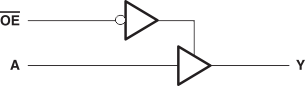
The SN74LVC1G125-Q1 device is a single line driver with a 3-state output. The output is disabled when the output-enable ( OE) input is high.
The CMOS device has high output drive while maintaining low static power dissipation over a broad VCC operating range.
The SN74LVC1G125-Q1 device is available in a variety of packages including the small DRY package with a body size of 1.45 mm × 1.00 mm.
Device Information
| DEVICE NAME | PACKAGE(1) | BODY SIZE (NOM) |
|---|---|---|
| CLVC1G125QDBVRQ1 | SOT-23 (5) | 2.90 mm × 1.60 mm |
| 1P1G125QDCKRQ1 | SC70 (5) | 2.00 mm × 1.25 mm |
| 1P1G125QDRYRQ1 | SON (6) | 1.45 mm × 1.00 mm |
(1) For all available packages, see the orderable addendum at the
end of the data sheet.