SCES424M January 2003 – August 2022 SN74LVC1G3157
PRODUCTION DATA
- 1 Features
- 2 Applications
- 3 Description
- 4 Revision History
- 5 Pin Configuration and Functions
- 6 Specifications
- 7 Parameter Measurement Information
- 8 Detailed Description
- 9 Application and Implementation
- 10Power Supply Recommendations
- 11Layout
- 12Device and Documentation Support
- 13Mechanical, Packaging, and Orderable Information
3 Description
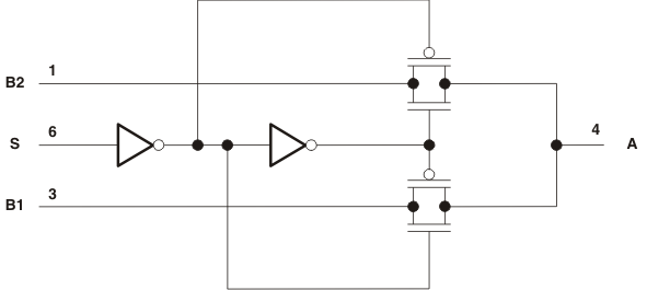
This single channel single-pole double-throw (SPDT) analog switch is designed for 1.65-V to 5.5-V VCC operation.
The SN74LVC1G3157 device can handle both analog and digital signals. The SN74LVC1G3157 device permits signals with amplitudes of up to VCC (peak) to be transmitted in either direction.
Applications include signal gating, chopping, modulation or demodulation (modem), and signal multiplexing for analog-to-digital and digital-to-analog conversion systems.
Device Information(1)
| PART NUMBER | PACKAGE | BODY SIZE (NOM) |
|---|---|---|
| SN74LVC1G3157 | SOT-23 (DBV) (6) | 2.90 mm × 1.60 mm |
| SC70 (DCK) (6) | 2.00 mm × 1.25 mm | |
| SOT (DRL) (6) | 1.60 mm × 1.20 mm | |
| SON (DRY) (6) | 1.45 mm × 1.00 mm | |
| DSBGA (YZP) (6) | 1.41 mm × 0.91 mm | |
| SON (DSF) (6) | 1.00 mm × 1.00 mm | |
| X2SON (DTB) (6) | 0.80 mm × 1.00 mm |
(1) For all available packages, see the orderable addendum at the end of the data sheet.
 Simplified Schematic