SCES929A January 2022 – May 2022 SN74LXC2T45-Q1
PRODUCTION DATA
- 1 Features
- 2 Applications
- 3 Description
- 4 Revision History
- 5 Pin Configuration and Functions
-
6 Specifications
- 6.1 Absolute Maximum Ratings
- 6.2 ESD Ratings
- 6.3 Recommended Operating Conditions
- 6.4 Thermal Information
- 6.5 Electrical Characteristics
- 6.6 Switching Characteristics: Tsk, TMAX
- 6.7 Switching Characteristics, VCCA = 1.2 ± 0.1 V
- 6.8 Switching Characteristics, VCCA = 1.5 ± 0.1 V
- 6.9 Switching Characteristics, VCCA = 1.8 ± 0.15 V
- 6.10 Switching Characteristics, VCCA = 2.5 ± 0.2 V
- 6.11 Switching Characteristics, VCCA = 3.3 ± 0.3 V
- 6.12 Switching Characteristics, VCCA = 5.0 ± 0.5 V
- 6.13 Operating Characteristics
- 6.14 Typical Characteristics
- 7 Parameter Measurement Information
-
8 Detailed Description
- 8.1 Overview
- 8.2 Functional Block Diagram
- 8.3
Feature Description
- 8.3.1 CMOS Schmitt-Trigger Inputs with Integrated Pulldowns
- 8.3.2 Balanced High-Drive CMOS Push-Pull Outputs
- 8.3.3 Partial Power Down (Ioff)
- 8.3.4 VCC Isolation and VCC Disconnect (Ioff-float)
- 8.3.5 Over-Voltage Tolerant Inputs
- 8.3.6 Glitch-Free Power Supply Sequencing
- 8.3.7 Negative Clamping Diodes
- 8.3.8 Fully Configurable Dual-Rail Design
- 8.3.9 Supports High-Speed Translation
- 8.4 Device Functional Modes
- 9 Application and Implementation
- 10Power Supply Recommendations
- 11Layout
- 12Device and Documentation Support
- 13Mechanical, Packaging, and Orderable Information
Package Options
Refer to the PDF data sheet for device specific package drawings
Mechanical Data (Package|Pins)
- DCU|8
- DTT|8
Thermal pad, mechanical data (Package|Pins)
Orderable Information
3 Description
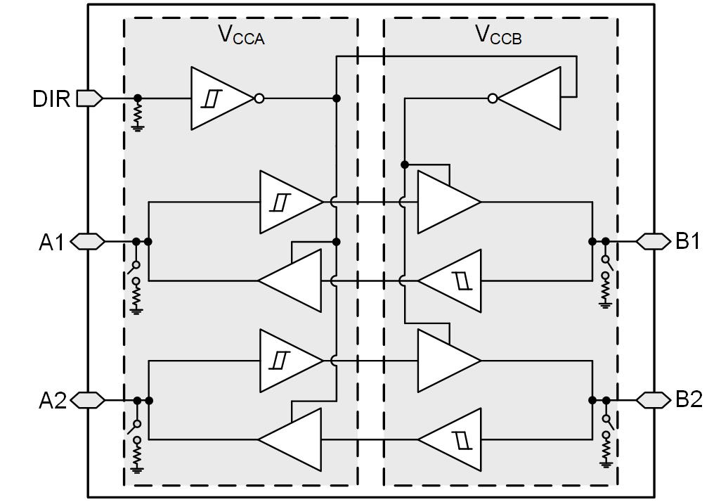
The SN74LXC2T45-Q1 is a dual-bit, dual-supply noninverting bidirectional voltage level translation device. Ax pins and control pin (DIR) are referenced to VCCA logic levels, and Bx pins are referenced to VCCB logic levels. The A port is able to accept I/O voltages ranging from 1.1 V to 5.5 V, while the B port can accept I/O voltages from 1.1 V to 5.5 V. A high on DIR allows data transmission from A to B and a low on DIR allows data transmission from B to A. See Device Functional Modes for a summary of the operation of the control logic.
Device Information(1)
| PART NUMBER | PACKAGE | BODY SIZE (NOM) |
|---|---|---|
| SN74LXC2T45-Q1 | VSSOP (DCU) (8) | 2.30 mm × 2.00 mm |
| SON (DTT) (8) | 1.95 mm × 1.00 mm |
(1) For all available packages, see the orderable addendum at the end of the data sheet.
 Functional Block Diagram