SCES625A February 2005 – November 2015 SN74VMEH22501A-EP
PRODUCTION DATA.
- 1 Features
- 2 Applications
- 3 Description
- 4 Revision History
- 5 Description (continued)
- 6 Pin Configuration and Functions
-
7 Specifications
- 7.1 Absolute Maximum Ratings
- 7.2 ESD Ratings
- 7.3 Recommended Operating Conditions
- 7.4 Thermal Information
- 7.5 Electrical Characteristics
- 7.6 Live-Insertion Specifications
- 7.7 Timing Requirements for UBT Transceiver (I Version)
- 7.8 Switching Characteristics for Bus Transceiver Function (I Version)
- 7.9 Switching Characteristics for Bus Transceiver Function (M Version)
- 7.10 Switching Characteristics for UBT Transceiver (I Version)
- 7.11 Switching Characteristics for UBT Transceiver (M Version)
- 7.12 Switching Characteristics for Bus Transceiver Function (I Version)
- 7.13 Switching Characteristics for UBT (I Version)
- 7.14 Switching Characteristics for Bus Transceiver Function (I Version)
- 7.15 Switching Characteristics for UBT (I Version)
- 7.16 Skew Characteristics for Bus Transceiver (I Version)
- 7.17 Skew Characteristics for Bus Transceiver (M Version)
- 7.18 Skew Characteristics for UBT (I Version)
- 7.19 Skew Characteristics for UBT (M Version)
- 7.20 Skew Characteristics for Bus Transceiver (I Version)
- 7.21 Skew Characteristics for UBT (I Version)
- 7.22 Skew Characteristics for Bus Transceiver (I Version)
- 7.23 Skew Characteristics for UBT (I Version)
- 7.24 Maximum Data Transfer Rates
- 7.25 Typical Characteristics
- 8 Parameter Measurement Information
- 9 Detailed Description
- 10Application and Implementation
- 11Power Supply Recommendations
- 12Layout
- 13Device and Documentation Support
- 14Mechanical, Packaging, and Orderable Information
Package Options
Mechanical Data (Package|Pins)
Thermal pad, mechanical data (Package|Pins)
Orderable Information
8 Parameter Measurement Information
8.1 Distributed-Load Backplane Switching Characteristics
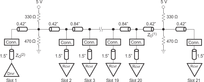
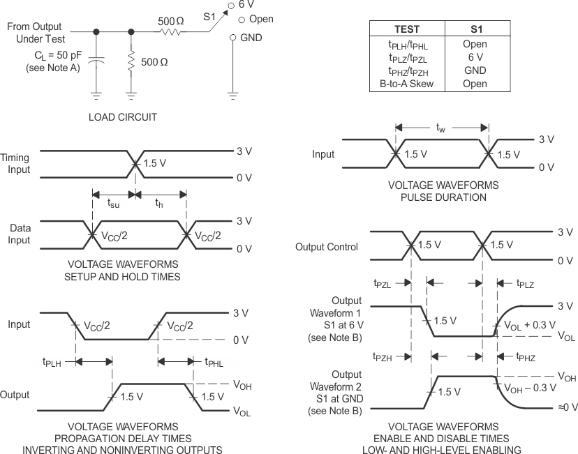
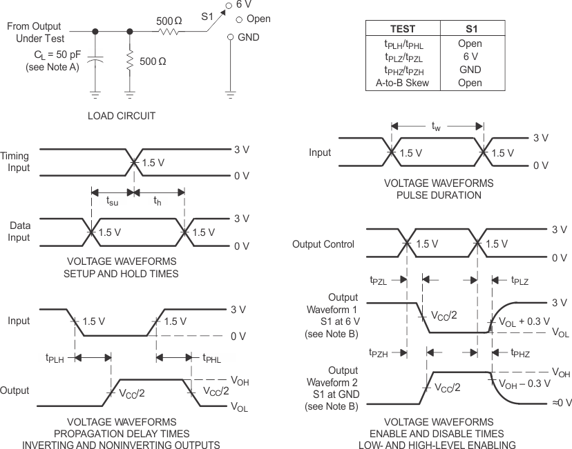
The switching characteristics tables show the switching characteristics of the device into the lumped load shown in this section (see Figure 7 and Figure 8). All logic devices currently are tested into this type of load. However, the designer's backplane application probably is a distributed load. For this reason, this device has been designed for optimum performance in the VME64x backplane as shown in Figure 6.

- Unloaded backplane trace natural impedance (ZO) is 45 Ω. 45 Ω to 60 Ω is allowed, with 50 Ω being ideal.
- Card stub natural impedance (ZO) is 60 Ω.
The following switching characteristics tables derived from TI-SPICE models show the switching characteristics of the device into the backplane under full and minimum loading conditions, to help the designer better understand the performance of the VME device in this typical backplane.

Waveform 2 is for an output with internal conditions such that the output is high, except when disabled by the output control.

Waveform 2 is for an output with internal conditions such that the output is high, except when disabled by the output control.