SLASEM6E october 2017 – july 2023 TAS2770
PRODUCTION DATA
- 1
- 1 Features
- 2 Applications
- 3 Description
- 4 Revision History
- 5 Pin Configuration and Functions
- 6 Specifications
- 7 Parameter Measurement Information
-
8 Detailed Description
- 8.1 Overview
- 8.2 Functional Block Diagram
- 8.3 Feature Description
- 8.4 Device Functional Modes
- 8.5
Register Maps
- 8.5.1 Register Summary Table Book=0x00 Page=0x00
- 8.5.2
Register Maps
- 8.5.2.1 PAGE (book=0x00 page=0x00 address=0x00) [reset=0h]
- 8.5.2.2 SW_RESET (book=0x00 page=0x00 address=0x01) [reset=0h]
- 8.5.2.3 PWR_CTL (book=0x00 page=0x00 address=0x02) [reset=Eh]
- 8.5.2.4 PB_CFG0 (book=0x00 page=0x00 address=0x03) [reset=10h]
- 8.5.2.5 PB_CFG1 (book=0x00 page=0x00 address=0x04) [reset=1h]
- 8.5.2.6 PB_CFG2 (book=0x00 page=0x00 address=0x05) [reset=0h]
- 8.5.2.7 PB_CFG3 (book=0x00 page=0x00 address=0x06) [reset=0h]
- 8.5.2.8 MISC_CFG (book=0x00 page=0x00 address=0x07) [reset=6h]
- 8.5.2.9 PDM_CFG0 (book=0x00 page=0x00 address=0x08) [reset=0h]
- 8.5.2.10 PDM_CFG1 (book=0x00 page=0x00 address=0x09) [reset=8h]
- 8.5.2.11 TDM_CFG0 (book=0x00 page=0x00 address=0x0A) [reset=7h]
- 8.5.2.12 TDM_CFG1 (book=0x00 page=0x00 address=0x0B) [reset=2h]
- 8.5.2.13 TDM_CFG2 (book=0x00 page=0x00 address=0x0C) [reset=Ah]
- 8.5.2.14 TDM_CFG3 (book=0x00 page=0x00 address=0x0D) [reset=10h]
- 8.5.2.15 TDM_CFG4 (book=0x00 page=0x00 address=0x0E) [reset=13h]
- 8.5.2.16 TDM_CFG5 (book=0x00 page=0x00 address=0x0F) [reset=2h]
- 8.5.2.17 TDM_CFG6 (book=0x00 page=0x00 address=0x10) [reset=0h]
- 8.5.2.18 TDM_CFG7 (book=0x00 page=0x00 address=0x11) [reset=4h]
- 8.5.2.19 TDM_CFG8 (book=0x00 page=0x00 address=0x12) [reset=6h]
- 8.5.2.20 TDM_CFG9 (book=0x00 page=0x00 address=0x13) [reset=7h]
- 8.5.2.21 TDM_CFG10 (book=0x00 page=0x00 address=0x14) [reset=8h]
- 8.5.2.22 LIM_CFG0 (book=0x00 page=0x00 address=0x15) [reset=14h]
- 8.5.2.23 LIM_CFG1 (book=0x00 page=0x00 address=0x16) [reset=76h]
- 8.5.2.24 LIM_CFG2 (book=0x00 page=0x00 address=0x17) [reset=10h]
- 8.5.2.25 LIM_CFG3 (book=0x00 page=0x00 address=0x18) [reset=6Eh]
- 8.5.2.26 LIM_CFG4 (book=0x00 page=0x00 address=0x19) [reset=1Eh]
- 8.5.2.27 LIM_CFG5 (book=0x00 page=0x00 address=0x1A) [reset=58h]
- 8.5.2.28 BOP_CFG0 (book=0x00 page=0x00 address=0x1B) [reset=1h]
- 8.5.2.29 BOP_CFG1 (book=0x00 page=0x00 address=0x1C) [reset=14h]
- 8.5.2.30 BOP_CFG2 (book=0x00 page=0x00 address=0x1D) [reset=4Eh]
- 8.5.2.31 ICLA_CFG0 (book=0x00 page=0x00 address=0x1E) [reset=0h]
- 8.5.2.32 ICLA_CFG1 (book=0x00 page=0x00 address=0x1F) [reset=0h]
- 8.5.2.33 INT_MASK0 (book=0x00 page=0x00 address=0x20) [reset=FCh]
- 8.5.2.34 INT_MASK1 (book=0x00 page=0x00 address=0x21) [reset=B1h]
- 8.5.2.35 INT_LIVE0 (book=0x00 page=0x00 address=0x22) [reset=0h]
- 8.5.2.36 INT_LIVE1 (book=0x00 page=0x00 address=0x23) [reset=0h]
- 8.5.2.37 INT_LTCH0 (book=0x00 page=0x00 address=0x24) [reset=0h]
- 8.5.2.38 INT_LTCH1 (book=0x00 page=0x00 address=0x25) [reset=0h]
- 8.5.2.39 INT_LTCH2 (book=0x00 page=0x00 address=0x26) [reset=0h]
- 8.5.2.40 VBAT_MSB (book=0x00 page=0x00 address=0x27) [reset=0h]
- 8.5.2.41 VBAT_LSB (book=0x00 page=0x00 address=0x28) [reset=0h]
- 8.5.2.42 TEMP_MSB (book=0x00 page=0x00 address=0x29) [reset=0h]
- 8.5.2.43 TEMP_LSB (book=0x00 page=0x00 address=0x2A) [reset=0h]
- 8.5.2.44 INT_CFG (book=0x00 page=0x00 address=0x30) [reset=5h]
- 8.5.2.45 DIN_PD (book=0x00 page=0x00 address=0x31) [reset=0h]
- 8.5.2.46 MISC_IRQ (book=0x00 page=0x00 address=0x32) [reset=81h]
- 8.5.2.47 CLOCK_CFG (book=0x00 page=0x00 address=0x3C) [reset=Dh]
- 8.5.2.48 TDM_DET (book=0x00 page=0x00 address=0x77) [reset=7Fh]
- 8.5.2.49 REV_ID (book=0x00 page=0x00 address=0x7D) [reset=20h]
- 8.5.2.50 I2C_CKSUM (book=0x00 page=0x00 address=0x7E) [reset=0h]
- 8.5.2.51 BOOK (book=0x00 page=0x00 address=0x7F) [reset=0h]
-
9 Application and Implementation
- 9.1 Application Information
- 9.2 Typical Application
- 9.3
Initialization Set Up
- 9.3.1 Initial Device Configuration - Auto Rate
- 9.3.2 Initial Device Configuration - 48 kHz
- 9.3.3 Initial Device Configuration - 44.1 kHz
- 9.3.4 Sample Rate Change - 48 kHz to 44.1kHz
- 9.3.5 Sample Rate Change - 44.1 kHz to 48 kHz
- 9.3.6 Device Mute
- 9.3.7 Device Un-Mute
- 9.3.8 Device Sleep
- 9.3.9 Device Wake
- 10Power Supply Recommendations
- 11Layout
- 12Device and Documentation Support
- 13Mechanical, Packaging, and Orderable Information
Package Options
Mechanical Data (Package|Pins)
Thermal pad, mechanical data (Package|Pins)
Orderable Information
3 Description
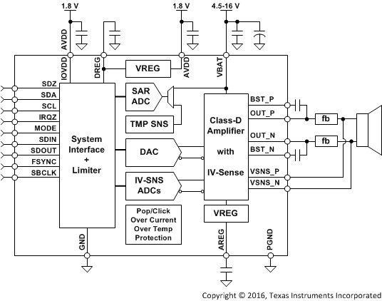
The TAS2770 is a mono, digital input Class-D audio amplifier optimized for efficiently driving small loudspeakers . The output power, protection features and packages make TAS2770 a good choice for Smart speakers, Bluetooth speakers, home automation devices, Notebook computers and tablets.
The Class-D amplifier is capable of delivering 20W of continuous power into a 4-Ω load at 16V and 15W into an 8-Ω load at 16V both at 1% THD. The broad voltage input range of 4.5-16V and the high output power makes this amplifier versatile enough to work with battery power or with line powered systems
A Brown-Out preventer tracks peak voltage and automatically self-limits the gain to the voltage available. This hardware implemented feature reduces the amplifier’s demand on system power preventing both audio cut out and system shutdown
The TAS2770 can be used as a conventional amp or with host based speaker protection algorithms. The integrated speaker voltage and current sense provides for real time feedback of loudspeaker conditions to the protection algorithms through a return I2S path.
Up to eight devices can share a common bus via either I2S/TDM + I2C.
The TAS2770 device is available in a 26-pin, 0.4-mm pitch QFN for a compact PCB footprint.
| PART NUMBER | PACKAGE | BODY SIZE (NOM) |
|---|---|---|
| TAS2770 | QFN | 4 mm × 3.5 mm |
| TAS2770 | DSBGA | 2 mm × 2.52 mm |
| SNP002770 | QFN | 4 mm × 3.5 mm |
| SNP002770 | DSBGA | 2 mm × 2.52 mm |
| TAS5770LC0 | DSBGA | 2 mm × 2.52 mm |
 Functional Block Diagram