SLAS623A November 2008 – November 2016 TAS5342A
PRODUCTION DATA.
- 1 Features
- 2 Applications
- 3 Description
- 4 Revision History
- 5 Pin Configuration and Functions
- 6 Specifications
-
7 Detailed Description
- 7.1 Overview
- 7.2 Functional Block Diagram
- 7.3
Feature Description
- 7.3.1 Mid Z Sequence Compatibility
- 7.3.2 Device Protection System
- 7.3.3 Use Of TAS5342A In High-Modulation-Index Capable Systems
- 7.3.4 Overcurrent (OC) Protection With Current Limiting and Overload Detection
- 7.3.5 Pin-To-Pin Short Circuit Protection System (PPSC)
- 7.3.6 Overtemperature Protection
- 7.3.7 Undervoltage Protection (UVP) and Power-On Reset (POR)
- 7.3.8 Error Reporting
- 7.3.9 Device Reset
- 7.4 Device Functional Modes
- 8 Application and Implementation
- 9 Power Supply Recommendations
- 10Layout
- 11Device and Documentation Support
- 12Mechanical, Packaging, and Orderable Information
Package Options
Mechanical Data (Package|Pins)
- DDV|44
Thermal pad, mechanical data (Package|Pins)
- DDV|44
Orderable Information
6 Specifications
6.1 Absolute Maximum Ratings
over operating free-air temperature range unless otherwise noted (1)| MIN | MAX | UNIT | ||
|---|---|---|---|---|
| VDD to AGND | –0.3 | 13.2 | V | |
| GVDD_X to AGND | –0.3 | 13.2 | V | |
| PVDD_X to GND_X (2) | –0.3 | 53 | V | |
| OUT_X to GND_X (2) | –0.3 | 53 | V | |
| BST_X to GND_X (2) | –0.3 | 66.2 | V | |
| BST_X to GVDD_X (2) | –0.3 | 53 | V | |
| VREG to AGND | –0.3 | 4.2 | V | |
| GND_X to GND | –0.3 | 0.3 | V | |
| GND_X to AGND | –0.3 | 0.3 | V | |
| GND to AGND | –0.3 | 0.3 | V | |
| PWM_X, OC_ADJ, M1, M2, M3 to AGND | –0.3 | 4.2 | V | |
| RESET_X, SD, OTW to AGND | –0.3 | 7 | V | |
| Maximum continuous sink current (SD, OTW) | 9 | mA | ||
| Minimum pulse duration, low | 30 | ns | ||
| Maximum operating junction temperature range, TJ | 0 | 125 | °C | |
| Storage temperature, Tstg | –40 | 125 | °C |
(1) Stresses beyond those listed under Absolute Maximum Ratings may cause permanent damage to the device. These are stress ratings only, and functional operation of the device at these or any other conditions beyond those indicated under Recommended Operating Conditions is not implied. Exposure to absolute-maximum-rated conditions for extended periods may affect device reliability.
(2) These voltages represent the DC voltage + peak AC waveform measured at the terminal of the device in all conditions.
6.2 ESD Ratings
| VALUE | UNIT | |||
|---|---|---|---|---|
| V(ESD) | Electrostatic discharge | Human-body model (HBM), per ANSI/ESDA/JEDEC JS-001(1) | ±2500 | V |
| Charged-device model (CDM), per JEDEC specification JESD22-C101(2) | ±750 | |||
(1) JEDEC document JEP155 states that 500-V HBM allows safe manufacturing with a standard ESD control process.
(2) JEDEC document JEP157 states that 250-V CDM allows safe manufacturing with a standard ESD control process.
6.3 Recommended Operating Conditions
over operating free-air temperature range (unless otherwise noted)| MIN | NOM | MAX | UNIT | |||
|---|---|---|---|---|---|---|
| PVDD_X | Half-bridge supply voltage | 0 | 31.5 | 34 | V | |
| GVDD_X | Supply voltage for logic regulators and gate-drive circuitry | 10.8 | 12 | 13.2 | V | |
| VDD | Digital regulator supply voltage | 10.8 | 12 | 13.2 | V | |
| RL (BTL) | Resistive load impedance (no Cycle-by-Cycle current control), recommended demodulation filter | 3 | 4 | Ω | ||
| RL (SE) | 2.25 | 3 | ||||
| RL (PBTL) | 1.5 | 2 | ||||
| LOutput (BTL) | Output-filter inductance | Minimum output inductance under short-circuit condition | 5 | 10 | μH | |
| LOutput (SE) | 5 | 10 | ||||
| LOutput (PBTL) | 5 | 10 | ||||
| fS | PWM frame rate | 192 | 384 | 432 | kHz | |
| tLOW | Minimum low-state pulse duration per PWM Frame, noise shaper enabled | 30 | nS | |||
| CPVDD | PVDD close decoupling capacitors | 0.1 | μF | |||
| CBST | Bootstrap capacitor, selected value supports PWM frame rates from 192 kHz to 432 kHz | 33 | nF | |||
| ROC | Over-current programming resistor | Resistor tolerance = 5% | 27 | 27 | 47 | kΩ |
| REXT-PULLUP | External pull-up resistor to 3.3 V to 5. 0 V for SD or OTW | 3.3 | 4.7 | kΩ | ||
| TJ | Junction temperature | 0 | 125 | °C | ||
6.4 Thermal Information
| THERMAL METRIC(1) | TAS5342A | UNIT | |
|---|---|---|---|
| DDV (HTSSOP) | |||
| 44 PINS | |||
| RθJA | Junction-to-ambient thermal resistance | 41.1 | °C/W |
| RθJC(top) | Junction-to-case (top) thermal resistance | 0.7 | °C/W |
| RθJB | Junction-to-board thermal resistance | 18.0 | °C/W |
| ψJT | Junction-to-top characterization parameter | 0.7 | °C/W |
| ψJB | Junction-to-board characterization parameter | 17.9 | °C/W |
| RθJC(bot) | Junction-to-case (bottom) thermal resistance | N/A | °C/W |
(1) For more information about traditional and new thermal metrics, see the Semicoductor and IC Package Thermal Metrics application report.
6.5 Electrical Characteristics
PVDD_x = 31.5 V, GVDD_X = 12 V, VDD = 12 V, TC (Case temperature) = 25°C, fS = 384 kHz, unless otherwise specified.| PARAMETER | TEST CONDITIONS | MIN | TYP | MAX | UNIT | |
|---|---|---|---|---|---|---|
| INTERNAL VOLTAGE REGULATOR AND CURRENT CONSUMPTION | ||||||
| VREG | Voltage regulator, only used as a reference node | VDD = 12 V | 3 | 3.3 | 3.6 | V |
| IVDD | VDD supply current | Operating, 50% duty cycle | 7.2 | 17 | mA | |
| Idle, reset mode | 5.54 | 11 | ||||
| IGVDD_X | Gate supply current per half-bridge | 50% duty cycle | 8 | 16 | mA | |
| Reset mode | 1 | 1.8 | ||||
| IPVDD_X | Half-bridge idle current | 50% duty cycle, with 10 µH and 470 nF output filter | 16.3 | 25 | mA | |
| Reset mode, no switching | 465 | 558 | μA | |||
| OUTPUT STAGE MOSFETS | ||||||
| RDSon,LS | Drain-to-source resistance, Low Side | TJ = 25°C, excludes metallization resistance, | 80 | 89 | mΩ | |
| RDSon,HS | Drain-to-source resistance, High Side | TJ = 25°C, excludes metallization resistance, | 80 | 89 | mΩ | |
| I/O PROTECTION | ||||||
| Vuvp,G | Undervoltage protection limit, GVDD_X | 9.5 | V | |||
| Vuvp,hyst (1) | Undervoltage protection limit, GVDD_X | 250 | mV | |||
| BSTuvpF | Puts device into RESET when BST voltage falls below limit | 5.85 | V | |||
| BSTuvpR | Brings device out of RESET when BST voltage rises above limit | 7 | V | |||
| OTW(1) | Overtemperature warning | 115 | 125 | 135 | °C | |
| OTWHYST (1) | Temperature drop needed below OTW temp. for OTW to be inactive after the OTW event | 25 | °C | |||
| OTE(1) | Overtemperature error threshold | 145 | 155 | 165 | °C | |
| OTE-OTWdifferential (1) | OTE - OTW differential, temperature delta between OTW and OTE | 30 | °C | |||
| OLPC | Overload protection counter | fS = 384 kHz | 1.25 | ms | ||
| IOC | Overcurrent limit protection | Resistor—programmable, high-end, ROC = 27 kΩ with 1 ms pulse | 10.1 | A | ||
| IOCT | Overcurrent response time | 150 | ns | |||
| tACTIVITY DETECTOR | Time for PWM activity detector to activite when no PWM is present | Lack of transistion of any PWM input | 13.2 | μS | ||
| IPD | Output pulldown current of each half-bridge | Connected when RESET is active to provide bootstrap capacitor charge. Not used in SE mode. | 3 | mA | ||
| STATIC DIGITAL SPECIFICATIONS | ||||||
| VIH | High-level input voltage | PWM_A, PWM_B, PWM_C, PWM_D, M1, M2, M3, RESET_AB, RESET_CD | 2 | V | ||
| VIL | Low-level input voltage | 0.8 | V | |||
| ILeakage | Input leakage current | 100 | μA | |||
| OTW/SHUTDOWN (SD) | ||||||
| RINT_PU | Internal pullup resistance, OTW to VREG, SD to VREG | 20 | 26 | 32 | kΩ | |
| VOH | High-level output voltage | Internal pullup resistor | 3 | 3.3 | 3.6 | V |
| External pullup of 4.7 kΩ to 5 V | 4.5 | 5 | ||||
| VOL | Low-level output voltage | IO = 4 mA | 0.2 | 0.4 | V | |
| FANOUT | Device fanout OTW, SD | No external pullup | 30 | Devices | ||
(1) Specified by design
6.6 Audio Specifications (BTL)
Audio performance is recorded as a chipset consisting of a TAS5518 pwm processor (modulation index limited to 97.7%) and a TAS5342A power stage. PCB and system configuration are in accordance with recommended guidelines. Audio frequency = 1 kHz, PVDD_x = 31.5 V, GVDD_x = 12 V, RL = 4 Ω, fS = 384 kHz, ROC = 27 kΩ, TC = 75°C, Output Filter: LDEM = 10 μH, CDEM = 470 nF, unless otherwise noted.| PARAMETER | TEST CONDITIONS | MIN | TYP | MAX | UNIT | |
|---|---|---|---|---|---|---|
| POMAX | Maximum Power Output | RL = 4 Ω, 10% THD+N, clipped input signal | 100 | W | ||
| RL = 6 Ω, 10% THD+N, clipped input signal | 80 | |||||
| RL = 8 Ω, 10% THD+N, clipped input signal | 65 | |||||
| PO | Unclipped Power Output | RL = 4 Ω, 0 dBFS, unclipped input signal | 80 | |||
| RL = 6 Ω, 0 dBFS, unclipped input signal | 64 | |||||
| RL = 8 Ω, 0 dBFS, unclipped input signal | 50 | |||||
| THD+N | Total harmonic distortion + noise | 0 dBFS; AES17 filter | 0.4% | |||
| 1 W; AES17 filter | 0.09% | |||||
| Vn | Output integrated noise | A-weighted, AES17 filter, Auto mute disabled | 45 | μV | ||
| SNR | Signal-to-noise ratio (1) | A-weighted, AES17 filter, Auto mute disabled | 110 | dB | ||
| DNR | Dynamic range | A-weighted, input level = –60 dBFS, AES17 filter | 110 | dB | ||
| DC Offset | Output offset voltage | ±15 | mV | |||
| Pidle | Power dissipation due to idle losses (IPVDD_X) | PO = 0 W, all halfbridges switching(2) | 2 | W | ||
(1) SNR is calculated relative to 0-dBFS input level.
(2) Actual system idle losses are affected by core losses of output inductors.
6.7 Audio Specifications (Single-Ended Output)
Audio performance is recorded as a chipset consisting of a TAS5086 pwm processor (modulation index limited to 97.7%) and a TAS5342A power stage. PCB and system configuration are in accordance with recommended guidelines. Audio frequency = 1 kHz, PVDD_x = 31.5 V, GVDD_x = 12 V, RL = 4 Ω, fS = 384 kHz, ROC = 27 kΩ, TC = 75°C, Output Filter: LDEM = 20 μH, CDEM = 1 μF, unless otherwise noted.| PARAMETER | TEST CONDITIONS | MIN | TYP | MAX | UNIT | |
|---|---|---|---|---|---|---|
| POMAX | Maximum Power Output | RL = 3 Ω, 10% THD+N, clipped input signal | 40 | W | ||
| RL = 4 Ω, 10% THD+N, clipped input signal | 30 | |||||
| PO | Unclipped Power Output | RL = 3 Ω, 0 dBFS, unclipped input signal | 30 | |||
| RL = 4 Ω, 0 dBFS, unclipped input signal | 20 | |||||
| THD+N | Total harmonic distortion + noise | 0 dBFS; AES17 filter | 0.2% | |||
| 1 W; AES17 filter | 0.1% | |||||
| Vn | Output integrated noise | A-weighted, AES17 filter, Auto mute disabled | 35 | μV | ||
| SNR | Signal-to-noise ratio(1) | A-weighted, AES17 filter, Auto mute disabled | 109 | dB | ||
| DNR | Dynamic range | A-weighted, input level = –60 dBFS AES17 filter | 109 | dB | ||
| Pidle | Power dissipation due to idle losses (IPVDD_X) | PO = 0 W, all half bridges switching(2) | 2 | W | ||
(1) SNR is calculated relative to 0-dBFS input level.
(2) Actual system idle losses are affected by core losses of output inductors.
6.8 Audio Specifications (PBTL)
Audio performance is recorded as a chipset consisting of a TAS5518 pwm processor (modulation index limited to 97.7%) and a TAS5342A power stage. PCB and system configuration are in accordance with recommended guidelines. Audio frequency = 1 kHz, PVDD_x = 31.5 V, GVDD_x = 12 V, RL = 3 Ω, fS = 384 kHz, ROC = 27 kΩ, TC = 75°C, Output Filter: LDEM = 10 μH, CDEM = 1 uF, unless otherwise noted.| PARAMETER | TEST CONDITIONS | MIN | TYP | MAX | UNIT | |
|---|---|---|---|---|---|---|
| POMAX | Maximum Power Output | RL = 2 Ω, 10% THD+N, clipped input signal | 200 | W | ||
| RL = 3 Ω, 10% THD+N, clipped input signal | 160 | |||||
| PO | Unclipped Power Output | RL = 2 Ω, 0 dBFS, unclipped input signal | 150 | |||
| RL = 3 Ω, 0 dBFS, unclipped input signal | 120 | |||||
| THD+N | Total harmonic distortion + noise | 0 dBFS; AES17 filter | 0.4% | |||
| 1 W; AES17 filter | 0.09% | |||||
| Vn | Output integrated noise | A-weighted, AES17 filter, Auto mute disabled | 45 | μV | ||
| SNR | Signal-to-noise ratio(1) | A-weighted, AES17 filter, Auto mute disabled | 110 | dB | ||
| DNR | Dynamic range | A-weighted, input level = –60 dBFS AES17 filter | 110 | dB | ||
| DC Offset | Output offset voltage | ±15 | mV | |||
| Pidle | Power dissipation due to idle losses (IPVDD_X) | PO = 0 W, all half bridges switching(2) | 2 | W | ||
(1) SNR is calculated relative to 0-dBFS input level.
(2) Actual system idle losses are affected by core losses of output inductors.
6.9 Typical Characteristics
6.9.1 BTL Configuration
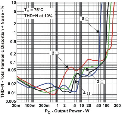
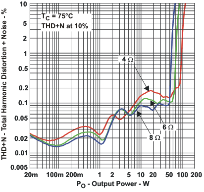 Figure 1. Total Harmonic Distortion + Noise vs Output Power
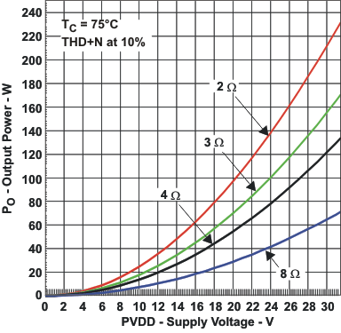
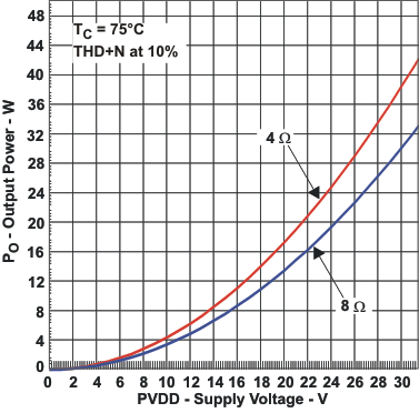
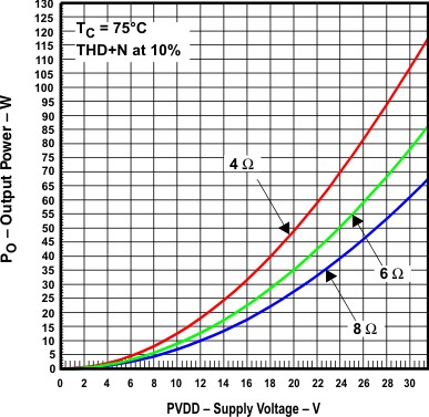 Figure 2. Output Power vs Supply Voltage
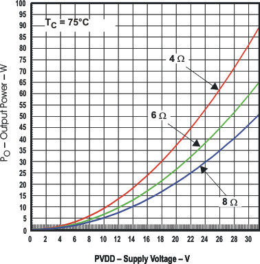 Figure 3. Unclipped Output Power vs Supply Voltage
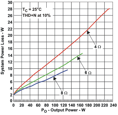 Figure 5. System Power Loss vs Output Power
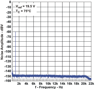 Figure 7. Noise Amplitude vs Frequency
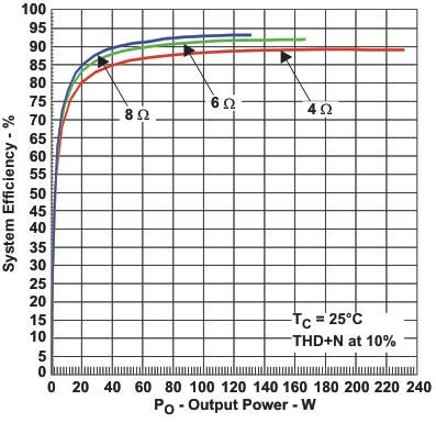 Figure 4. System Efficiency vs Output Power
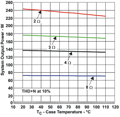
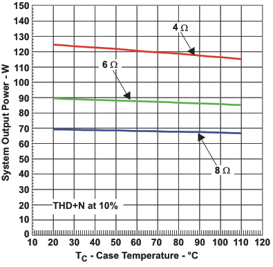 Figure 6. System Output Power vs Case Temperature
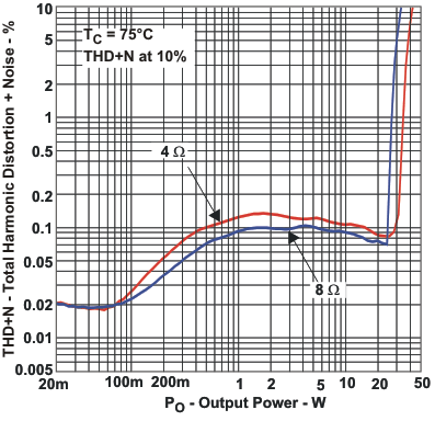
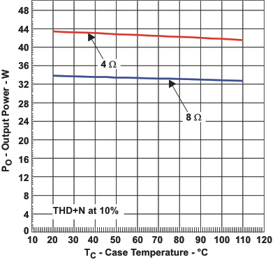
6.9.2 SE Configuration
6.9.3 PBTL Configuration
