SLOS955 December 2016 TAS5414C
PRODUCTION DATA.
- 1 Features
- 2 Applications
- 3 Description
- 4 Revision History
- 5 Pin Configuration and Functions
- 6 Specifications
-
7 Detailed Description
- 7.1 Overview
- 7.2 Functional Block Diagram
- 7.3 Feature Descption
- 7.4 Device Functional Modes
- 7.5 Programming
- 7.6
Register Maps
- 7.6.1 Register Summary
- 7.6.2 Registers
- 7.6.3 Fault Register 2 (0x01) Protection
- 7.6.4 Diagnostic Register 1 (0x02) Load Diagnostics
- 7.6.5 Diagnostic Register 2 (0x03) Load Diagnostics
- 7.6.6 External Status Register 1 (0x04) Fault Detection
- 7.6.7 External Status Register 2 (0x05) Output State of Individual Channels
- 7.6.8 External Status Register 3 (0x06) Play and Mute Modes
- 7.6.9 External Status Register 4 (0x07) Load Diagnostics
- 7.6.10 External Control Register 1 (0x08) Gain Select
- 7.6.11 External Control Register 2 (0x09) Overcurrent Control
- 7.6.12 External Control Register 3 (0x0A) Switching Frequency Select and Clip_OTW Configuration
- 7.6.13 External Control Register 4 (0x0B) Load Diagnostics and Master/Slave Control
- 7.6.14 External Control Register 5 (0x0C) Output Control
- 7.6.15 External Control Register 6 (0x0D) Output Control
- 7.6.16 External Control Register 7 (0x10) Miscellaneous Selection
- 7.6.17 External Status Register 5 (0x13) Overtemperature and Thermal Foldback Status
- 8 Application and Implementation
- 9 Power Supply Recommendations
- 10Layout
- 11Device and Documentation Support
- 12Mechanical, Packaging, and Orderable Information
Package Options
Mechanical Data (Package|Pins)
- PHD|64
Thermal pad, mechanical data (Package|Pins)
- PHD|64
Orderable Information
1 Features
- Four-Channel Single-Ended Analog Input Class-D Audio Amplifier
- Typical Output Power at 10% THD+N
- 28 W/Ch Into 4 Ω at 14.4 V
- 50 W/Ch Into 2 Ω at 14.4 V
- 79 W/Ch Into 4 Ω at 24 V
- 150 W/Ch Into 2 Ω at 24 V (PBTL)
- Channels Can Be Paralleled (PBTL) for High-Current Applications
- THD+N < 0.02%, 1 kHz, 1 W Into 4 Ω
- Patented Pop- and Click-Reduction Technology
- Soft Muting With Gain Ramp Control
- Common-Mode Ramping
- Patented AM Interference Avoidance
- Patented Cycle-by-Cycle Current Limit
- 75-dB PSRR
- Four-Address I2C Serial Interface for Device Configuration and Control
- Channel Gains: 12-dB, 20-dB, 26-dB, 32-dB
- Load Diagnostic Functions:
- Output Open and Shorted Load
- Output-to-Power and -to-Ground Shorts
- Patented Tweeter Detection
- Protection and Monitoring Functions:
- Short-Circuit Protection
- Load-Dump Protection to 50 V
- Fortuitous Open-Ground and -Power Tolerant
- Patented Output DC Level Detection While Music Playing
- Overtemperature Protection
- Over- and Undervoltage Conditions
- Clip Detection
- 64-Pin QFP (PHD) Power Package With Heat Slug Up
- –20°C to 105°C Ambient Temperature Range
2 Applications
- Aftermarket Headunit
- Aftermarket External Audio Amplifier
3 Description
The TAS5414C is a four-channel Class-D audio amplifier designed for use in automotive head units and external amplifier modules. It provides four channels at 23 W continuously into 4 Ω at less than 1% THD+N from a 14.4-V supply. Each channel can also deliver 38 W into 2 Ω at 1% THD+N. The TAS5414C uses single-ended analog inputs. The class-D PWM topology of the device provides dramatic improvements in efficiency over traditional linear amplifier solutions. This reduces the power dissipated by the amplifier by a factor of ten under typical music playback conditions. The device has a built-in load diagnostic functions for detecting and diagnosing misconnected outputs to help to reduce test time during the manufacturing process.
Device Information(1)
| PART NUMBER | PACKAGE | BODY SIZE (NOM) |
|---|---|---|
| TAS5414C | HTQFP (64) | 14.00 mm × 14.00 mm |
- For all available packages, see the orderable addendum at the end of the datasheet.
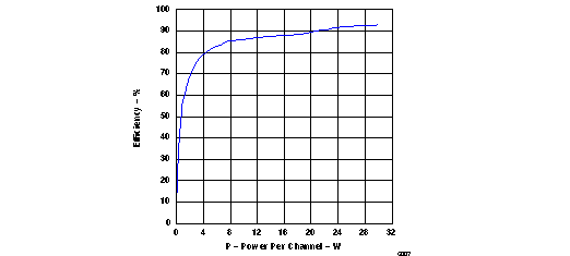
Efficiency vs Power Per Channel

4 Revision History
| DATE | REVISION | NOTES |
|---|---|---|
| December 2016 | * | Initial release. |