SLASEC1B March 2016 – May 2018 TAS5751M
PRODUCTION DATA.
- 1 Features
- 2 Applications
- 3 Description
- 4 Revision History
- 5 Pin Configuration and Functions
-
6 Specifications
- 6.1 Absolute Maximum Ratings
- 6.2 ESD Ratings
- 6.3 Recommended Operating Conditions
- 6.4 Thermal Characteristics
- 6.5 Electrical Characteristics
- 6.6 Speaker Amplifier Characteristics
- 6.7 Protection Characteristics
- 6.8 Master Clock Characteristics
- 6.9 I²C Interface Timing Requirements
- 6.10 Serial Audio Port Timing Requirements
- 6.11 Typical Characteristics
-
7 Detailed Description
- 7.1 Overview
- 7.2 Functional Block Diagram
- 7.3 Audio Signal Processing Overview
- 7.4 Feature Description
- 7.5 Device Functional Modes
- 7.6 Programming
- 7.7
Register Maps
- 7.7.1 Register Summary
- 7.7.2
Detailed Register Descriptions
- 7.7.2.1 Clock Control Register (0x00)
- 7.7.2.2 Device ID Register (0x01)
- 7.7.2.3 Error Status Register (0x02)
- 7.7.2.4 System Control Register 1 (0x03)
- 7.7.2.5 Serial Data Interface Register (0x04)
- 7.7.2.6 System Control Register 2 (0x05)
- 7.7.2.7 Soft Mute Register (0x06)
- 7.7.2.8 Volume Registers (0x07, 0x08, 0x09)
- 7.7.2.9 Volume Configuration Register (0x0E)
- 7.7.2.10 Modulation Limit Register (0x10)
- 7.7.2.11 Interchannel Delay Registers (0x11, 0x12, 0x13, and 0x14)
- 7.7.2.12 PWM Shutdown Group Register (0x19)
- 7.7.2.13 Start/Stop Period Register (0x1A)
- 7.7.2.14 Oscillator Trim Register (0x1B)
- 7.7.2.15 BKND_ERR Register (0x1C)
- 7.7.2.16 Input Multiplexer Register (0x20)
- 7.7.2.17 PWM Output MUX Register (0x25)
- 7.7.2.18 AGL Control Register (0x46)
- 7.7.2.19 PWM Switching Rate Control Register (0x4F)
- 7.7.2.20 Bank Switch and EQ Control (0x50)
-
8 Application and Implementation
- 8.1 Application Information
- 8.2
Typical Applications
- 8.2.1
Stereo Bridge Tied Load Application
- 8.2.1.1 Design Requirements
- 8.2.1.2 Detailed Design Procedure
- 8.2.1.3 Application Performance Plots
- 8.2.2 Mono Parallel Bridge Tied Load Application
- 8.2.1
Stereo Bridge Tied Load Application
- 9 Power Supply Recommendations
- 10Layout
- 11Device and Documentation Support
- 12Mechanical, Packaging, and Orderable Information
Package Options
Mechanical Data (Package|Pins)
- DCA|48
Thermal pad, mechanical data (Package|Pins)
- DCA|48
Orderable Information
7.4.5 Headphone/Line Amplifier
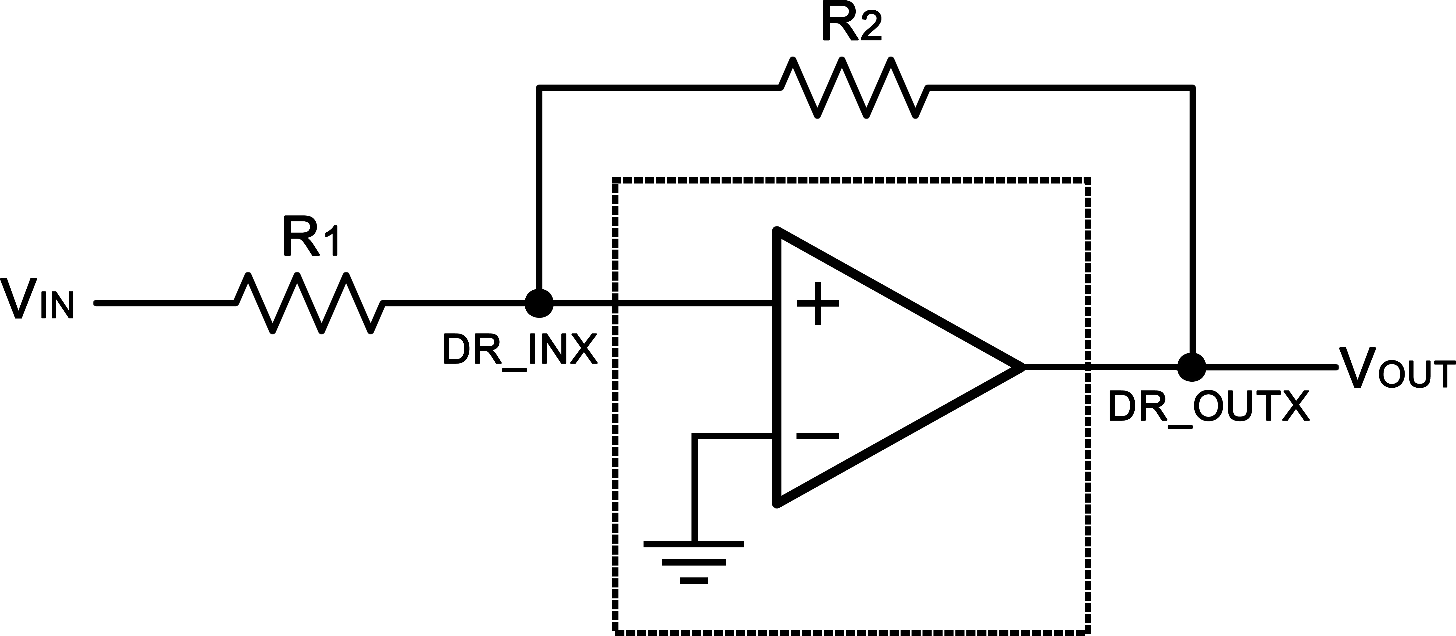
An integrated ground centered DirectPath combination headphone amplifier and line driver is integrated in the TAS5729MD. This headphone/line amplifier can be used independently from the device speaker amplifier modes, with analog single-ended inputs DR_INA and DR_INB, linked to the respective analog outputs DR_OUTA, and DR_OUTB. A basic diagram of the headphone/line amplifier is shown in Figure 49.
 Figure 49. Headphone/Line Amplifier
 The DR_SDI pin can be used to turn on or off the headphone amplifier and line driver. The DirectPath amplifier makes use of the provided positive and negative supply rails generated by the IC. The output voltages are centered at zero volts with the capability to swing to the positive rail or negative rail; combining this capability with the built-in click and pop reduction circuit, the DirectPath amplifier requires no output dc blocking capacitors.