SCPS234A September   2016  – February 2023 TCA6408A-Q1

PRODUCTION DATA  

  1. Features
  2. Applications
  3. Description
  4. Revision History
  5. Pin Configuration and Functions
  6. Specifications
    1. 6.1 Absolute Maximum Ratings
    2. 6.2 ESD Ratings
    3. 6.3 Recommended Operating Conditions
    4. 6.4 Thermal Information
    5. 6.5 Electrical Characteristics
    6. 6.6 I2C Interface Timing Requirements
    7. 6.7 Reset Timing Requirements
    8. 6.8 Switching Characteristics
    9. 6.9 Typical Characteristics
  7. Parameter Measurement Information
  8. Detailed Description
    1. 8.1 Overview
    2. 8.2 Functional Block Diagrams
    3. 8.3 Feature Description
      1. 8.3.1 Voltage Translation
      2. 8.3.2 I/O Port
      3. 8.3.3 Interrupt Output ( INT)
      4. 8.3.4 Reset Input ( RESET)
    4. 8.4 Device Functional Modes
      1. 8.4.1 Power-On Reset (POR)
      2. 8.4.2 Powered-Up
    5. 8.5 Programming
      1. 8.5.1 I2C Interface
      2. 8.5.2 Bus Transactions
        1. 8.5.2.1 Writes
        2. 8.5.2.2 Reads
    6. 8.6 Register Map
      1. 8.6.1 Device Address
      2. 8.6.2 Control Register and Command Byte
      3. 8.6.3 Register Descriptions
  9. Application and Implementation
    1. 9.1 Application Information
    2. 9.2 Typical Application
      1. 9.2.1 Design Requirements
        1. 9.2.1.1 Calculating Junction Temperature and Power Dissipation
        2. 9.2.1.2 Minimizing ICC When I/O is Used to Control LEDs
      2. 9.2.2 Detailed Design Procedure
      3. 9.2.3 Application Curves
    3. 9.3 Power Supply Recommendations
      1. 9.3.1 Power-On Reset Requirements
    4. 9.4 Layout
      1. 9.4.1 Layout Guidelines
      2. 9.4.2 Layout Example
  10. 10Device and Documentation Support
    1. 10.1 Receiving Notification of Documentation Updates
    2. 10.2 Trademarks
    3. 10.3 Electrostatic Discharge Caution
    4. 10.4 Glossary
  11. 11Support Resources
  12. 12Mechanical, Packaging, and Orderable Information

Package Options

Mechanical Data (Package|Pins)
Thermal pad, mechanical data (Package|Pins)
Orderable Information

Detailed Design Procedure

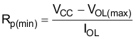
The pull-up resistors, RP, for the SCL and SDA lines need to be selected appropriately and take into consideration the total capacitance of all targets on the I2C bus. The minimum pull-up resistance is a function of VCC, VOL,(max), and IOL as shown in Equation 5.

Equation 5. GUID-ACBF6E48-D699-4B25-A96A-6B984B716809-low.gif

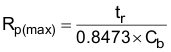
The maximum pull-up resistance is a function of the maximum rise time, tr (300 ns for fast-mode operation,
fSCL = 400 kHz) and bus capacitance, Cb as shown in Equation 6.

Equation 6. GUID-0D86981B-0D5C-4DF9-B189-1F174B35DFC7-low.gif

The maximum bus capacitance for an I2C bus must not exceed 400 pF for standard-mode or fast-mode operation. The bus capacitance can be approximated by adding the capacitance of the TCA6408A-Q1, Ci for SCL or CIO for SDA, the capacitance of wires, connections, traces, and the capacitance of additional targets on the bus.