SCPS272C October 2019 – January 2021 TCA9511A
PRODUCTION DATA
- 1 Features
- 2 Applications
- 3 Description
- 4 Revision History
- 5 Pin Configuration and Functions
- 6 Specifications
- 7 Parameter Measurement Information
- 8 Detailed Description
- 9 Application Information Disclaimer
- 10Power Supply Recommendations
- 11Layout
- 12Device and Documentation Support
- 13Mechanical, Packaging, and Orderable Information
Package Options
Mechanical Data (Package|Pins)
- DGK|8
Thermal pad, mechanical data (Package|Pins)
- DGK|8
Orderable Information
9.2.1.2 Multiple connections to a common node
It is possible to have multiple buffers in connect to a common node, but care must be taken when designing a system.
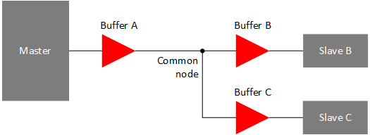
 Figure 9-3 Connections to Common Node
It is important to try and avoid common node architectures. The multiple nodes sharing a common node can create glitches if the output voltage from a master slave device plus the offset voltage of the buffer are high enough to trip the RTA. Also keep in mind that the VOS must be crossed in order for a device to begin to regulate the other side.
Consider a system with three buffers connected to a common node and communication between the Master and Slave B that are connected at either end of buffer A and buffer B in series as shown in Figure 9-3. Consider if the VOL at the input of buffer A is 0.3 V and the VOL of Slave B (when acknowledging) is 0.36 V with the direction changing from Master to Slave B and then from Slave B to Master. Before the direction change the user should observe VIL at the input of buffer A of 0.3 V and its output, the common node, is ~0.36 V. The output of buffer B and buffer C would be ~0.42 V, but Slave B is driving 0.4 V, so the voltage at Slave B is 0.4 V. The output of buffer C is ~0.52 V. When the Master pull-down turns off, the input of buffer A rises and so does its output, the common node, because it is the only part driving the node. The common node rises to ~0.5 V before the buffer B output turns on, if the pull-up is strong the node may bounce. If the bounce goes above the threshold for the rising edge accelerator ~0.6 V, the accelerators on both buffer A and buffer C will fire, contending with the output of buffer B. The node on the input of buffer A goes high as will the input node of buffer C. After the common node voltage is stable for a while, the rising edge accelerators turn off, and the common node returns to ~0.5 V because the buffer B is still on. The voltage at both the Master and Slave C nodes then fall to ~0.6 V until Slave B turned off. This does not cause a failure on the data line as long as the return to 0.5 V on the common node (~0.56 V at the Master and Slave C) occurred before the data setup time. If this were the SCL line, the parts on buffer A and buffer C would see a false clock rather than a stretched clock, which causes a system error.