SCPS245C December 2012 – December 2018 TCA9517A
PRODUCTION DATA.
- 1 Features
- 2 Applications
- 3 Description
- 4 Revision History
- 5 Description (continued)
- 6 Pin Configuration and Functions
- 7 Specifications
- 8 Parameter Measurement Information
- 9 Detailed Description
- 10Application and Implementation
- 11Power Supply Recommendations
- 12Layout
- 13Device and Documentation Support
- 14Mechanical, Packaging, and Orderable Information
Package Options
Mechanical Data (Package|Pins)
- DGK|8
Thermal pad, mechanical data (Package|Pins)
- DGK|8
Orderable Information
10.2.2.2 VILC and Pullup Resistor Sizing
For the TCA9517A to function correctly, all devices on the B-side must be able to pull the B-side below the voltage input low contention level (VILC). This means that the VOL of any device on the B-side must be below
0.45 V.
VOL of a device can be adjusted by changing the IOL through the device which is set by the pull-up resistance value. The pull-up resistance on the B-side must be carefully selected to ensure that logic levels will be transferred correctly to the A-side.
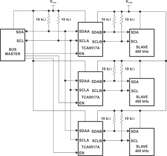
 Figure 8. Typical Star Application
 Multiple A sides of TCA9517As can be connected in a star configuration, allowing all nodes to communicate with each other.
 Figure 9. Typical Series Application
 To further extend the I2C bus for long traces/cables, multiple TCA9517As can be connected in series as long as the A-side is connected to the B-side. I2C bus slave devices can be connected to any of the bus segments. The number of devices that can be connected in series is limited by repeater delay/time-of-flight considerations on the maximum bus speed requirements.
 Figure 10. Bus A (0.9 V to 5.5 V Bus) Waveform
  Figure 11. Bus B (2.7 V to 5.5 V Bus) Waveform