SCPS207G May 2012 – November 2019 TCA9548A
PRODUCTION DATA.
- 1 Features
- 2 Applications
- 3 Description
- 4 Revision History
- 5 Pin Configuration and Functions
- 6 Specifications
- 7 Parameter Measurement Information
- 8 Detailed Description
- 9 Application and Implementation
- 10Power Supply Recommendations
- 11Layout
- 12Device and Documentation Support
- 13Mechanical, Packaging, and Orderable Information
Package Options
Mechanical Data (Package|Pins)
Thermal pad, mechanical data (Package|Pins)
- RGE|24
Orderable Information
8.5.2 Device Address
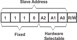
Figure 9 shows the address byte of the TCA9548A.
 Figure 9. TCA9548A Address
 The last bit of the slave address defines the operation (read or write) to be performed. When it is high (1), a read is selected, while a low (0) selects a write operation.
Table 1 shows the TCA9548A address reference.
Table 1. Address Reference
| INPUTS | I2C BUS SLAVE ADDRESS | ||
|---|---|---|---|
| A2 | A1 | A0 | |
| L | L | L | 112 (decimal), 70 (hexadecimal) |
| L | L | H | 113 (decimal), 71 (hexadecimal) |
| L | H | L | 114 (decimal), 72 (hexadecimal) |
| L | H | H | 115 (decimal), 73 (hexadecimal) |
| H | L | L | 116 (decimal), 74 (hexadecimal) |
| H | L | H | 117 (decimal), 75 (hexadecimal) |
| H | H | L | 118 (decimal), 76 (hexadecimal) |
| H | H | H | 119 (decimal), 77 (hexadecimal) |