SCPS207G May   2012  – November 2019 TCA9548A

PRODUCTION DATA.  

  1. Features
  2. Applications
  3. Description
    1.     Device Images
      1.      Simplified Application Diagram
  4. Revision History
  5. Pin Configuration and Functions
    1.     Pin Functions
  6. Specifications
    1. 6.1 Absolute Maximum Ratings
    2. 6.2 ESD Ratings
    3. 6.3 Recommended Operating Conditions
    4. 6.4 Thermal Information
    5. 6.5 Electrical Characteristics
    6. 6.6 I2C Interface Timing Requirements
    7. 6.7 Reset Timing Requirements
    8. 6.8 Switching Characteristics
    9. 6.9 Typical Characteristics
  7. Parameter Measurement Information
  8. Detailed Description
    1. 8.1 Overview
    2. 8.2 Functional Block Diagram
    3. 8.3 Feature Description
    4. 8.4 Device Functional Modes
      1. 8.4.1 RESET Input
      2. 8.4.2 Power-On Reset
    5. 8.5 Programming
      1. 8.5.1 I2C Interface
      2. 8.5.2 Device Address
      3. 8.5.3 Bus Transactions
        1. 8.5.3.1 Writes
        2. 8.5.3.2 Reads
      4. 8.5.4 Control Register
      5. 8.5.5 RESET Input
      6. 8.5.6 Power-On Reset
  9. Application and Implementation
    1. 9.1 Application Information
    2. 9.2 Typical Application
      1. 9.2.1 Design Requirements
      2. 9.2.2 Detailed Design Procedure
      3. 9.2.3 Application Curves
  10. 10Power Supply Recommendations
    1. 10.1 Power-On Reset Requirements
  11. 11Layout
    1. 11.1 Layout Guidelines
    2. 11.2 Layout Example
  12. 12Device and Documentation Support
    1. 12.1 Documentation Support
      1. 12.1.1 Related Documentation
    2. 12.2 Receiving Notification of Documentation Updates
    3. 12.3 Support Resources
    4. 12.4 Trademarks
    5. 12.5 Electrostatic Discharge Caution
    6. 12.6 Glossary
  13. 13Mechanical, Packaging, and Orderable Information

Package Options

Mechanical Data (Package|Pins)
Thermal pad, mechanical data (Package|Pins)
Orderable Information

Writes

To write on the I2C bus, the master sends a START condition on the bus with the address of the slave, as well as the last bit (the R/W bit) set to 0, which signifies a write. The slave acknowledges, letting the master know it is ready. After this, the master starts sending the control register data to the slave until the master has sent all the data necessary (which is sometimes only a single byte), and the master terminates the transmission with a STOP condition.

There is no limit to the number of bytes sent, but the last byte sent is what is in the register.

Figure 10 shows an example of writing a single byte to a slave register.
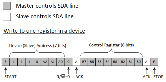
TCA9548A i2c_write.gifFigure 10. Write to Register