SCPS267B March 2017 – February 2020 TCA9803
PRODUCTION DATA.
- 1 Features
- 2 Applications
- 3 Description
- 4 Revision History
- 5 Device Comparison Table
- 6 Pin Configuration and Functions
- 7 Specifications
- 8 Parameter Measurement Information
-
9 Detailed Description
- 9.1 Overview
- 9.2 Functional Block Diagram
- 9.3
Feature Description
- 9.3.1 Integrated Current Source
- 9.3.2 Ultra-Low Power Consumption
- 9.3.3 No Static-Voltage Offset
- 9.3.4 Active-High Repeater Enable Input
- 9.3.5 Powered Off High Impedance I2C Bus Pins on A-Side
- 9.3.6 Powered-Off Back-Power Protection for I2C Bus Pins
- 9.3.7 Clock Stretching and Multiple Master Arbitration Support
- 9.4 Device Functional Modes
- 10Application and Implementation
- 11Power Supply Recommendations
- 12Layout
- 13Device and Documentation Support
- 14Mechanical, Packaging, and Orderable Information
Package Options
Mechanical Data (Package|Pins)
- DGK|8
Thermal pad, mechanical data (Package|Pins)
- DGK|8
Orderable Information
10.1.2.1 FET or Pass-Gate Translators
Some translators are based on pass-gates for translation support. In most of the use cases, external pull-up resistors are required to pull the bus to the voltage rail.
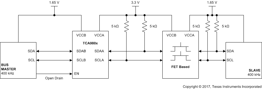
 Figure 15. Incorrect B-Side Pass-Gate Based Translator Use Case
  Figure 16. A-Side Pass-Gate Based Translator Use Case
 As shown in Figure 15, it may appear that this use case is valid, but actually it is not. When either the TCA980x B-side or the slave pull down on the bus, the FET isolating the bus closes (low RDS_ON) and current from the 5-kΩ resistor is observed by the TCA980x, violating IEXT-I. See the IEXT-I section for more information.
Figure 16 shows the correct way to pair with a FET base translator (connecting to the A-side).
Rather than using a FET-based translator, it is recommended that a buffered translator be used, such as another TCA980x or a TCA9517. See the Typical Application section for single device for more information on concerns with B-side connections to buffered translators.