SLLSES9D February 2016 – October 2021 TCAN1042-Q1 , TCAN1042G-Q1 , TCAN1042GV-Q1 , TCAN1042H-Q1 , TCAN1042HG-Q1 , TCAN1042HGV-Q1 , TCAN1042HV-Q1 , TCAN1042V-Q1
PRODUCTION DATA
- 1 Features
- 2 Applications
- 3 Description
- 4 Revision History
- 5 Device Comparison Table
- 6 Pin Configurations and Functions
- 7 Specifications
- 8 Parameter Measurement Information
-
9 Detailed Description
- 9.1 Overview
- 9.2 Functional Block Diagram
- 9.3 Feature Description
- 9.4 Device Functional Modes
- 10Application Information Disclaimer
- 11Power Supply Recommendations
- 12Device and Documentation Support
- 13Mechanical, Packaging, and Orderable Information
Package Options
Mechanical Data (Package|Pins)
Thermal pad, mechanical data (Package|Pins)
- DRB|8
Orderable Information
10.2.2.1 CAN Termination
The ISO 11898 standard specifies the interconnect to be a twisted pair cable (shielded or unshielded) with 120-Ω characteristic impedance (ZO). Resistors equal to the characteristic impedance of the line should be used to terminate both ends of the cable to prevent signal reflections. Unterminated drop lines (stubs) connecting nodes to the bus should be kept as short as possible to minimize signal reflections. The termination may be on the cable or in a node, but if nodes may be removed from the bus, the termination must be carefully placed so that two terminations always exist on the network.
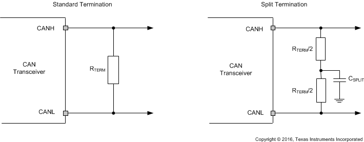
Termination may be a single 120-Ω resistor at the end of the bus, either on the cable or in a terminating node. If filtering and stabilization of the common mode voltage of the bus is desired, then split termination may be used. (See Figure 10-2). Split termination improves the electromagnetic emissions behavior of the network by eliminating fluctuations in the bus common-mode voltages at the start and end of message transmissions.
 Figure 10-2 CAN Bus Termination Concepts
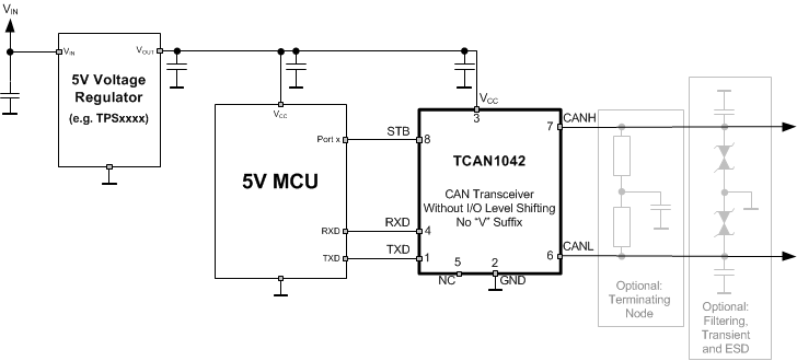
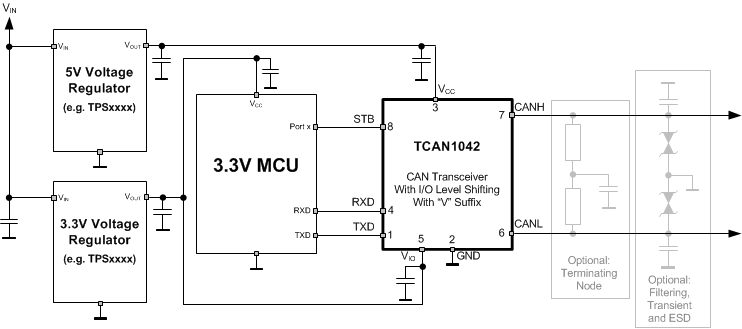
The family of transceivers have variants for both 5-V only applications and applications where level shifting is needed for a 3.3-V microcontroller.
 Figure 10-3 Typical CAN Bus Application Using 5V CAN Controller
 Figure 10-4 Typical CAN Bus Application Using 3.3 V CAN Controller