SLLSES9D February 2016 – October 2021 TCAN1042-Q1 , TCAN1042G-Q1 , TCAN1042GV-Q1 , TCAN1042H-Q1 , TCAN1042HG-Q1 , TCAN1042HGV-Q1 , TCAN1042HV-Q1 , TCAN1042V-Q1
PRODUCTION DATA
- 1 Features
- 2 Applications
- 3 Description
- 4 Revision History
- 5 Device Comparison Table
- 6 Pin Configurations and Functions
- 7 Specifications
- 8 Parameter Measurement Information
-
9 Detailed Description
- 9.1 Overview
- 9.2 Functional Block Diagram
- 9.3 Feature Description
- 9.4 Device Functional Modes
- 10Application Information Disclaimer
- 11Power Supply Recommendations
- 12Device and Documentation Support
- 13Mechanical, Packaging, and Orderable Information
Package Options
Mechanical Data (Package|Pins)
Thermal pad, mechanical data (Package|Pins)
- DRB|8
Orderable Information
9.4.3.1 Remote Wake Request via Wake Up Pattern (WUP) in Standby Mode
The family offers a remote wake request feature that is used to indicate to the host microcontroller that the bus is active and the node should return to normal operation.
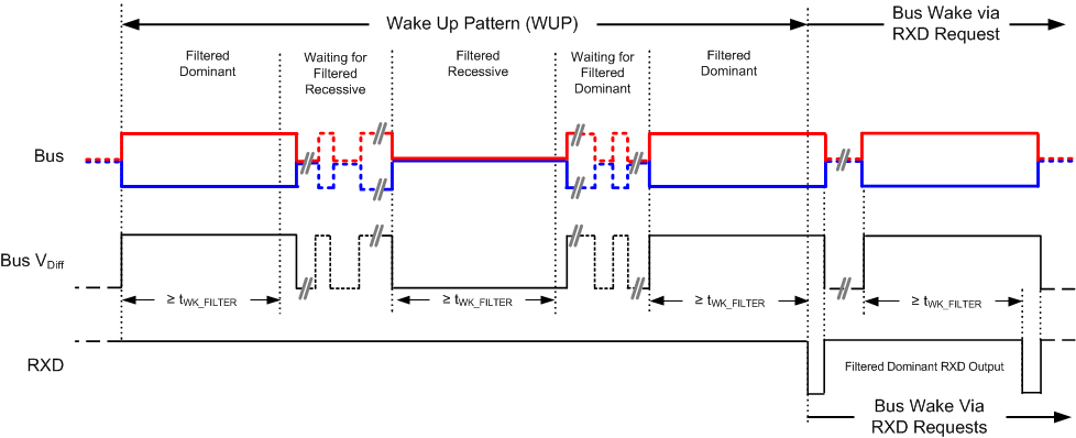
These devices use the multiple filtered dominant wake up pattern (WUP) from the ISO11898-2 (2016) to qualify bus activity. Once a valid WUP has been received the wake request will be indicated to the microcontroller by a falling edge and low corresponding to a "filtered" dominant on the RXD output terminal.
The WUP consists of a filtered dominant pulse, followed by a filtered recessive pulse, and finally by a second filtered dominant pulse. These filtered dominant, recessive, dominant pulses do not need to occur in immediate succession. There is no timeout that will occur between filtered bits of the WUP. Once a full WUP has been detected the device will continue to drive the RXD output low every time an additional filtered dominant signal is received from the bus.
For a dominant or recessive signal to be considered "filtered", the bus must continually remain in that state for more than tWK_FILTER. Due to variability in the tWK_FILTER, the following three scenarios can exist:
- Bus signals that last less than tWK_FILTER(MIN) will never be detected as part of a valid WUP
- Bus signals that last more than tWK_FILTER(MIN) but less than tWK_FILTER(MAX) may be detected as part of a valid WUP
- Bus signals that last more than tWK_FILTER(MAX) will always be detected as part of a valid WUP
Once the first filtered dominant signal is received, the device is now waiting on a filtered recessive signal, other bus traffic will not reset the bus monitor. Once the filtered recessive signal is received, the monitor is now waiting on a second filtered dominant signal, and again other bus traffic will not reset the monitor. After reception of the full WUP, the device will transition to driving the RXD output pin low for the remainder of any dominant signal that remains on the bus for longer than tWK_FILTER.
 Figure 9-4 Wake Up
Pattern (WUP)