SLLSEV0F November   2017  – November 2023 TCAN1043-Q1 , TCAN1043G-Q1 , TCAN1043H-Q1 , TCAN1043HG-Q1

PRODUCTION DATA  

  1.   1
  2. Features
  3. Applications
  4. Description
  5. Device Comparison Table
  6. Pin Configuration and Functions
  7. Specifications
    1. 6.1 Absolute Maximum Ratings
    2. 6.2 ESD Ratings
    3. 6.3 ESD Ratings IEC Specification
    4. 6.4 Recommended Operating Conditions
    5. 6.5 Thermal Information
    6. 6.6 Dissipation Ratings
    7. 6.7 Electrical Characteristics
    8. 6.8 Switching Characteristics
    9. 6.9 Typical Characteristics
  8. Parameter Measurement Information
  9. Detailed Description
    1. 8.1 Overview
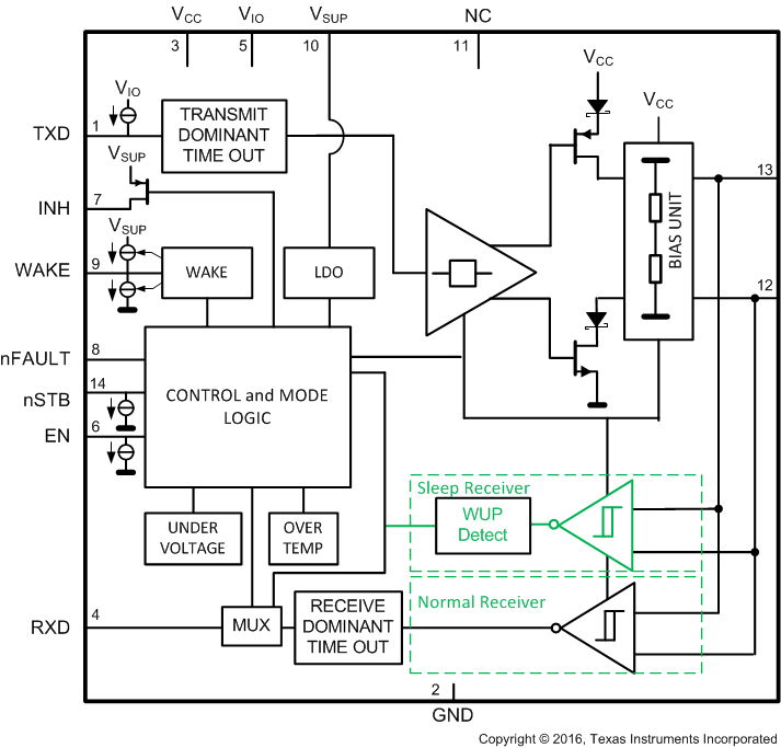
    2. 8.2 Functional Block Diagram
    3. 8.3 Feature Description
      1. 8.3.1 Internal and External Indicator Flags (nFAULT and RXD)
      2. 8.3.2 Power-Up Flag (PWRON)
      3. 8.3.3 Wake-Up Request Flag (WAKERQ)
      4. 8.3.4 Wake-Up Source Recognition Flag (WAKESR)
      5. 8.3.5 Undervoltage Fault Flags
        1. 8.3.5.1 Undervoltage on VCC Fault
        2. 8.3.5.2 Undervoltage on VIO Fault
        3. 8.3.5.3 Undervoltage on VSUP Fault
      6. 8.3.6 CAN Bus Failure Fault Flag
      7. 8.3.7 Local Faults
        1. 8.3.7.1 TXD Dominant Timeout (TXD DTO)
        2. 8.3.7.2 TXD Shorted to RXD Fault
        3. 8.3.7.3 CAN Bus Dominant Fault
        4. 8.3.7.4 Thermal Shutdown (TSD)
        5. 8.3.7.5 RXD Recessive Fault
        6. 8.3.7.6 Undervoltage Lockout (UVLO)
        7. 8.3.7.7 Unpowered Device
        8. 8.3.7.8 Floating Terminals
        9. 8.3.7.9 CAN Bus Short Circuit Current Limiting
    4. 8.4 Device Functional Modes
      1. 8.4.1 CAN Bus States
      2. 8.4.2 Normal Mode
      3. 8.4.3 Silent Mode
      4. 8.4.4 Standby Mode
      5. 8.4.5 Go-to-Sleep Mode
      6. 8.4.6 Sleep Mode with Remote Wake and Local Wake Up Requests
        1. 8.4.6.1 Remote Wake Request via Wake Up Pattern (WUP)
        2. 8.4.6.2 Local Wake Up (LWU) via WAKE Input Terminal
      7. 8.4.7 Driver and Receiver Function Tables
      8. 8.4.8 Digital Inputs and Outputs
      9. 8.4.9 INH (Inhibit) Output
  10. Application Information Disclaimer
    1. 9.1 Application Information
    2. 9.2 Typical Application
      1. 9.2.1 Design Requirements
        1. 9.2.1.1 Bus Loading, Length and Number of Nodes
      2. 9.2.2 Detailed Design Procedures
        1. 9.2.2.1 CAN Termination
      3. 9.2.3 Application Curves
    3. 9.3 Power Supply Recommendations
    4. 9.4 Layout
      1. 9.4.1 Layout
        1. 9.4.1.1 Layout Guidelines
      2. 9.4.2 Layout Example
  11. 10Device and Documentation Support
    1. 10.1 Receiving Notification of Documentation Updates
    2. 10.2 Support Resources
    3. 10.3 Trademarks
    4. 10.4 Electrostatic Discharge Caution
    5. 10.5 Glossary
  12. 11Revision History
  13. 12Mechanical, Packaging, and Orderable Information

Package Options

Mechanical Data (Package|Pins)
Thermal pad, mechanical data (Package|Pins)
Orderable Information

Description

The TCAN1043xx-Q1 meets the physical layer requirements of the ISO 11898–2 (2016) High Speed Controller Area Network (CAN) specification providing an interface between the CAN bus and the CAN protocol controller. These devices support both classical CAN and CAN FD up to 2 megabits per second (Mbps). Devices with part numbers that include the suffix “G” are designed for CAN FD data rates up to 5Mbps. The TCAN1043xx-Q1 allows for system-level reductions in battery current consumption by selectively enabling (via the INH output pin) the various power supplies that can be present on a node. This allows an ultra-low-current sleep state in which power is gated to all system components except for the TCAN1043xx-Q1, which remains in a low-power state monitoring the CAN bus.

When a wake-up pattern is detected on the bus or when a local wake-up is requested via the WAKE input, the TCAN1043xx-Q1 initiates node start-up by driving INH high. The TCAN1043xx-Q1 includes internal logic level translation via the VIO terminal to allow for interfacing directly to 3.3 V or 5 V controllers. The device includes many protection and diagnostic features including CAN bus line short-circuit detection and battery connection detection. The TCAN1043xx-Q1 meets the ESD and EMC requirements of IEC 62228-3 and J2962-2 without the need for additional protection components.

Package Information
PART NUMBER PACKAGE(1) PACKAGE SIZE(2)
TCAN1043xx-Q1 SOIC (14) 8.65 mm × 6 mm
VSON (14) 4.5 mm × 3 mm
For more information, see Section 12.
The package size (length × width) is a nominal value and includes pins, where applicable.
GUID-7F32F9D2-6DDA-4A16-B8C1-01C93E54A9FF-low.gif Functional Block Diagram