SLLSFL8A July 2021 – December 2021 TCAN1046AV-Q1 , TCAN1048AV-Q1
PRODUCTION DATA
- 1 Features
- 2 Applications
- 3 Description
- 4 Revision History
- 5 Description Continued
- 6 Device Comparison
- 7 Pin Configuration and Functions
- 8 Specifications
- 9 Parameter Measurement Information
-
10Detailed Description
- 10.1 Overview
- 10.2 Functional Block Diagram
- 10.3 Feature Description
- 10.4 Device Functional Modes
- 11Application and Implementation
- 12Power Supply Recommendations
- 13Layout
- 14Device and Documentation Support
- 15Mechanical, Packaging, and Orderable Information
Package Options
Mechanical Data (Package|Pins)
Thermal pad, mechanical data (Package|Pins)
Orderable Information
7 Pin Configuration and Functions
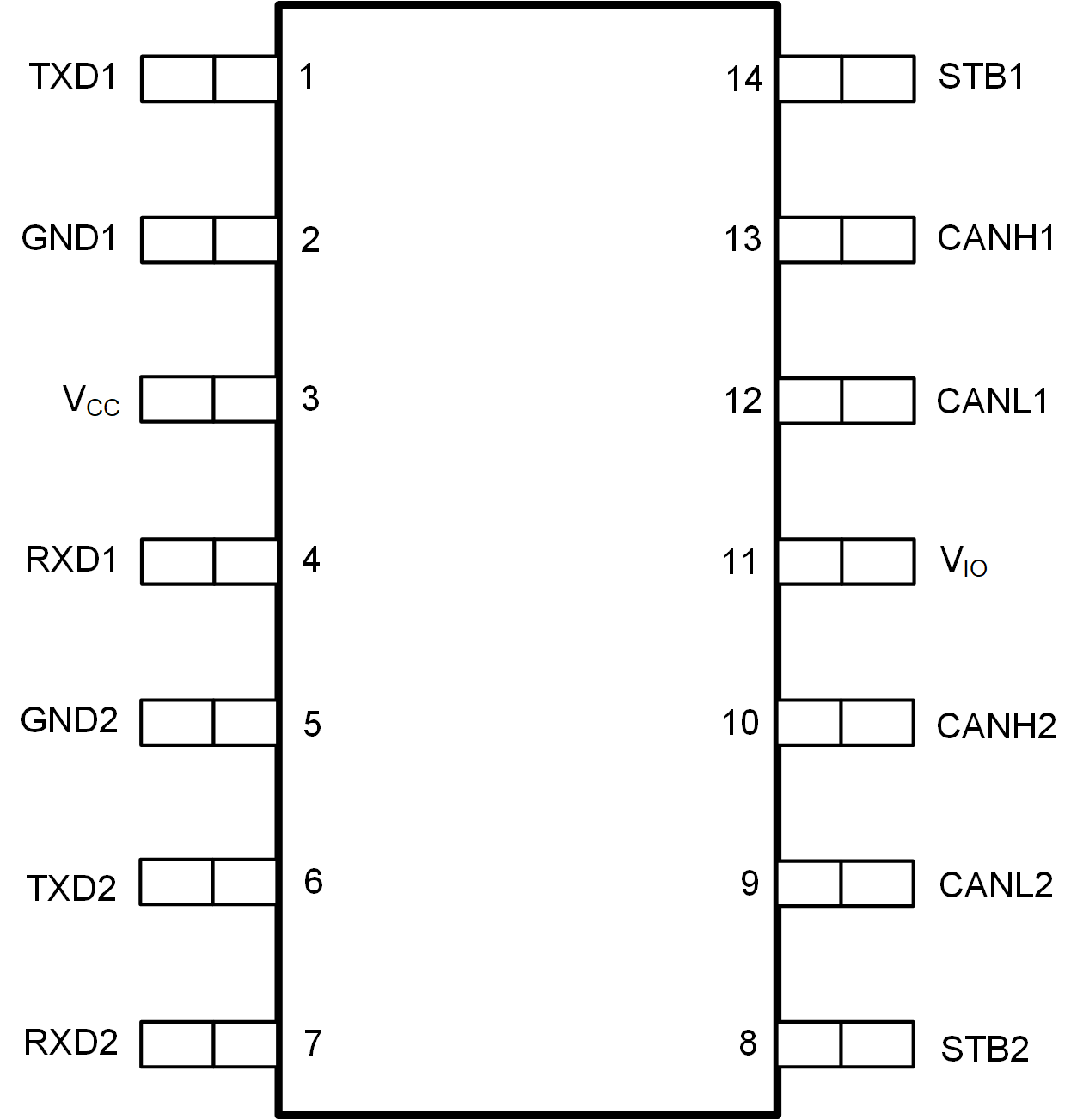
Figure 7-1 D Package, 14 Pin SOIC, Top View
Figure 7-3 DMT Package, 14 Pin VSON, Top View
 Figure 7-2 DYY Package, 14 Pin
SOT-23, Top View
Figure 7-2 DYY Package, 14 Pin
SOT-23, Top ViewTable 7-1 Pin Functions
| Pins | Type | Description | |
|---|---|---|---|
| Name | No. | ||
| TXD1 | 1 | Digital Input | CAN transmit data input channel 1; integrated pull-up |
| GND1 | 2 | GND | Ground connection |
| VCC | 3 | Supply | 5-V supply voltage |
| RXD1 | 4 | Digital Output | CAN receive data output channel 1; tri-state when VIO < UVVIO |
| GND2 | 5 | GND | Ground connection |
| TXD2 | 6 | Digital Input | CAN transmit data input channel 2; integrated pull-up |
| RXD2 | 7 | Digital Output | CAN receive data output channel 2; tri-state when VIO < UVVIO |
| STB2 | 8 | Digital Input | Standby input of channel 2 for mode control; integrated pull-up (TCAN1046AV–Q1) |
| nSTB2 | Standby input of channel 2 for mode control; inverse logic with integrated pull-down (TCAN1048AV–Q1) | ||
| CANL2 | 9 | Bus IO | Low-level CAN bus channel 2 input/output line |
| CANH2 | 10 | Bus IO | High-level CAN bus channel 2 input/output line |
| VIO | 11 | Supply | I/O supply voltage |
| CANL1 | 12 | Bus IO | Low-level CAN bus channel 1 input/output line |
| CANH1 | 13 | Bus IO | High-level CAN bus channel 1 input/output line |
| STB1 | 14 | Digital Input | Standby input of channel 1 for mode control; integrated pull-up (TCAN1046AV–Q1) |
| nSTB1 | Standby input of channel 1 for mode control; inverse logic with integrated pull-down (TCAN1048AV–Q1) | ||
| Thermal Pad (VSON only) | — | Connect the thermal pad to the printed circuit board (PCB) ground plane for thermal relief | |