SLLSF31A May   2021  – December 2021 TCAN1162-Q1

PRODUCTION DATA  

  1. Features
  2. Applications
  3. Description
  4. Revision History
  5. Description (continued)
  6. Pin Configurations and Functions
  7. Specifications
    1. 7.1 Absolute Maximum Ratings
    2. 7.2 ESD Ratings
    3. 7.3 ESD Ratings IEC Specification
    4. 7.4 Recomended Operating Conditions
    5. 7.5 Thermal Information
    6. 7.6 Power Supply Characteristics
    7. 7.7 Electrical Characteristics
    8. 7.8 Switching Characteristics
    9. 7.9 Typical Characteristics
  8. Parameter Measurement Information
  9. Detailed Description
    1. 9.1 Overview
    2. 9.2 Functional Block Diagram
    3. 9.3 Feature Description
      1. 9.3.1  VSUP Pin
      2. 9.3.2  VFLT Pin
      3. 9.3.3  Digital Inputs and Outputs
        1. 9.3.3.1 TXD Pin
        2. 9.3.3.2 RXD Pin
        3. 9.3.3.3 TS Pin
      4. 9.3.4  Digital Control and Timing
      5. 9.3.5  VIO Pin
      6. 9.3.6  GND
      7. 9.3.7  INH Pin
      8. 9.3.8  WAKE Pin
      9. 9.3.9  CAN Bus Pins
      10. 9.3.10 Local Faults
        1. 9.3.10.1 TXD Dominant Timeout (TXD DTO)
        2. 9.3.10.2 Thermal Shutdown (TSD)
        3. 9.3.10.3 Under/Over Voltage Lockout
        4. 9.3.10.4 Unpowered Devices
        5. 9.3.10.5 Floating Terminals
        6. 9.3.10.6 CAN Bus Short Circuit Current Limiting
        7. 9.3.10.7 Sleep Wake Error Timer
    4. 9.4 Device Functional Modes
      1. 9.4.1 Operating Mode Description
        1. 9.4.1.1 Normal Mode
        2. 9.4.1.2 Standby Mode
        3. 9.4.1.3 Sleep Mode
          1. 9.4.1.3.1 Remote Wake Request via Wake-Up Pattern (WUP)
          2. 9.4.1.3.2 Local Wake-Up (LWU) via WAKE Input Terminal
        4. 9.4.1.4 Fail-safe Mode
      2. 9.4.2 CAN Transceiver
        1. 9.4.2.1 CAN Transceiver Operation
        2. 9.4.2.2 CAN Transceiver Modes
          1. 9.4.2.2.1 CAN Off Mode
          2. 9.4.2.2.2 CAN Autonomous: Inactive and Active
          3. 9.4.2.2.3 CAN Active
        3. 9.4.2.3 Driver and Receiver Function Tables
        4. 9.4.2.4 CAN Bus States
  10. 10Application Information
    1. 10.1 Application Information Disclaimer
    2. 10.2 Typical Application
      1. 10.2.1 Design Requirements
        1. 10.2.1.1 Bus Loading, Length and Number of Nodes
      2. 10.2.2 Detailed Design Procedures
        1. 10.2.2.1 CAN Termination
    3. 10.3 Application Curves
  11. 11Power Supply Requirements
  12. 12Layout
    1. 12.1 Layout Guidelines
    2. 12.2 Layout Example
  13. 13Device and Documentation Support
    1. 13.1 Documentation Support
      1. 13.1.1 Related Documentation
    2. 13.2 Receiving Notification of Documentation Updates
    3. 13.3 Support Resources
    4. 13.4 Trademarks
    5. 13.5 Electrostatic Discharge Caution
    6. 13.6 Glossary
  14. 14Mechanical, Packaging, and Orderable Information

Package Options

Mechanical Data (Package|Pins)
Thermal pad, mechanical data (Package|Pins)
Orderable Information

Description

The TCAN1162-Q1 is a high-speed Controller Area Network (CAN) transceiver that meets the physical layer requirements of the ISO 11898-2:2016 high-speed CAN specification. The TCAN1162-Q1 supports both classical CAN and CAN FD networks up to 8 megabits per second (Mbps).

The TCAN1162-Q1 integrates a 5-V LDO with a wide input operating range which provides the CAN transceiver voltage thereby eliminating the need for the 5-V supply to be supplied from an external voltage source.

The TCAN1162-Q1 allows for system-level reductions in battery current consumption by selectively enabling the various power supplies that may be present on a system via the INH output pin. This allows an ultra-low-current sleep state where power is gated to all system components except for the TCAN1162-Q1, while monitoring the CAN bus. When a wake-up event is detected, the TCAN1162-Q1 initiates system start-up by driving INH high.

Device Information
PART NUMBER PACKAGE(1) BODY SIZE (NOM)
TCAN1162-Q1 VSON (14) 4.5 mm x 3.00 mm
For all available packages, see the orderable addendum at the end of the data sheet.
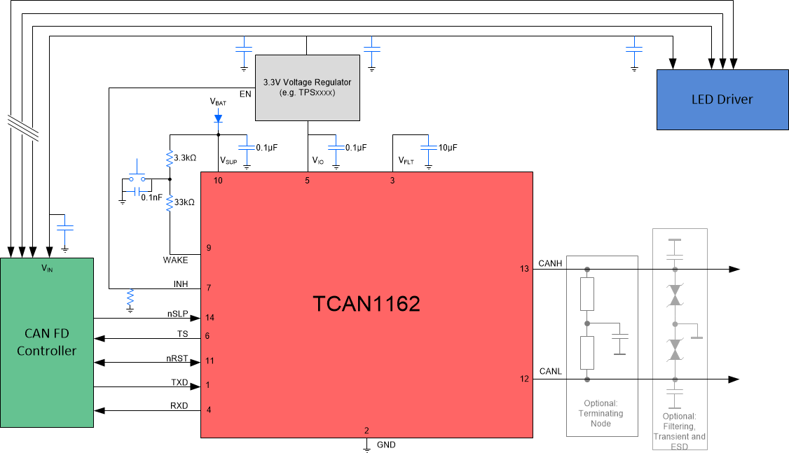
GUID-E45E8EDD-12AF-4851-B568-B50D0FB37D6B-low.gif Simplified Schematic