SLLSEQ7E December   2015  – December 2019 TCAN330 , TCAN330G , TCAN332 , TCAN332G , TCAN334 , TCAN334G , TCAN337 , TCAN337G

PRODUCTION DATA.  

  1. Features
  2. Applications
  3. Description
    1.     Block Diagram
  4. Revision History
  5. Description (continued)
  6. Device Options
  7. Pin Configuration and Functions
    1.     Pin Functions
  8. Specifications
    1. 8.1 Absolute Maximum Ratings
    2. 8.2 ESD Ratings
    3. 8.3 Recommended Operating Conditions
    4. 8.4 Thermal Information
    5. 8.5 Electrical Characteristics
    6. 8.6 Switching Characteristics
    7. 8.7 Typical Characteristics
    8. 8.8 Typical Characteristics, TCAN330 Receiver
    9. 8.9 Typical Characteristics, TCAN330 Driver
  9. Parameter Measurement Information
  10. 10Detailed Description
    1. 10.1 Overview
    2. 10.2 Functional Block Diagram
    3. 10.3 Feature Description
      1. 10.3.1 TXD Dominant Timeout (TXD DTO)
      2. 10.3.2 RXD Dominant Timeout (RXD DTO)
      3. 10.3.3 Thermal Shutdown
      4. 10.3.4 Undervoltage Lockout and Unpowered Device
      5. 10.3.5 Fault Pin (TCAN337)
      6. 10.3.6 Floating Pins
      7. 10.3.7 CAN Bus Short Circuit Current Limiting
      8. 10.3.8 ESD Protection
      9. 10.3.9 Digital Inputs and Outputs
    4. 10.4 Device Functional Modes
      1. 10.4.1 CAN Bus States
      2. 10.4.2 Normal Mode
      3. 10.4.3 Silent Mode
      4. 10.4.4 Standby Mode with Wake
      5. 10.4.5 Bus Wake via RXD Request (BWRR) in Standby Mode
      6. 10.4.6 Shutdown Mode
      7. 10.4.7 Driver and Receiver Function Tables
  11. 11Application and Implementation
    1. 11.1 Application Information
      1. 11.1.1 Bus Loading, Length and Number of Nodes
    2. 11.2 Typical Application
      1. 11.2.1 Design Requirements
        1. 11.2.1.1 CAN Termination
      2. 11.2.2 Detailed Design Procedure
      3. 11.2.3 Application Curves
    3. 11.3 System Examples
      1. 11.3.1 ISO11898 Compliance of TCAN33x Family of 3.3-V CAN Transceivers Introduction
      2. 11.3.2 Differential Signal
      3. 11.3.3 Common-Mode Signal and EMC Performance
  12. 12Power Supply Recommendations
  13. 13Layout
    1. 13.1 Layout Guidelines
    2. 13.2 Layout Example
  14. 14Device and Documentation Support
    1. 14.1 Related Links
    2. 14.2 Support Resources
    3. 14.3 Trademarks
    4. 14.4 Electrostatic Discharge Caution
    5. 14.5 Glossary
  15. 15Mechanical, Packaging, and Orderable Information

Package Options

Mechanical Data (Package|Pins)
Thermal pad, mechanical data (Package|Pins)
Orderable Information

Differential Signal

CAN is a differential bus where complementary signals are sent over two wires and the voltage difference between the two wires defines the logical state of the bus. The differential CAN receiver monitors this voltage difference and outputs the bus state with a single ended logic level output signal.
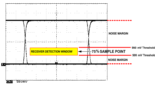
TCAN330 TCAN332 TCAN334 TCAN337 TCAN330G TCAN332G TCAN334G TCAN337G diff_pov_wf_sllseq7.gifFigure 39. Typical Differential Output Waveform

The CAN driver creates the differential voltage between CANH and CANL in the dominant state. The dominant differential output of the TCAN33x is greater than 1.5 V and less than 3 V across a 60-Ω load as defined by the ISO11898 standard. These are the same limiting values for 5 V supplied CAN transceivers. The bus termination resistors drive the recessive bus state and not the CAN driver.

A CAN receiver is required to output a recessive state when less than 500 mV of differential voltage exists on the bus, and a dominant state when more than 900 mV of differential voltage exists on the bus. The CAN receiver must do this with common-mode input voltages from –2 V to 7 V. The TCAN33x family receivers meet these same input specifications as 5 V supplied receivers.