SLLSEQ7E December   2015  – December 2019 TCAN330 , TCAN330G , TCAN332 , TCAN332G , TCAN334 , TCAN334G , TCAN337 , TCAN337G

PRODUCTION DATA.  

  1. Features
  2. Applications
  3. Description
    1.     Block Diagram
  4. Revision History
  5. Description (continued)
  6. Device Options
  7. Pin Configuration and Functions
    1.     Pin Functions
  8. Specifications
    1. 8.1 Absolute Maximum Ratings
    2. 8.2 ESD Ratings
    3. 8.3 Recommended Operating Conditions
    4. 8.4 Thermal Information
    5. 8.5 Electrical Characteristics
    6. 8.6 Switching Characteristics
    7. 8.7 Typical Characteristics
    8. 8.8 Typical Characteristics, TCAN330 Receiver
    9. 8.9 Typical Characteristics, TCAN330 Driver
  9. Parameter Measurement Information
  10. 10Detailed Description
    1. 10.1 Overview
    2. 10.2 Functional Block Diagram
    3. 10.3 Feature Description
      1. 10.3.1 TXD Dominant Timeout (TXD DTO)
      2. 10.3.2 RXD Dominant Timeout (RXD DTO)
      3. 10.3.3 Thermal Shutdown
      4. 10.3.4 Undervoltage Lockout and Unpowered Device
      5. 10.3.5 Fault Pin (TCAN337)
      6. 10.3.6 Floating Pins
      7. 10.3.7 CAN Bus Short Circuit Current Limiting
      8. 10.3.8 ESD Protection
      9. 10.3.9 Digital Inputs and Outputs
    4. 10.4 Device Functional Modes
      1. 10.4.1 CAN Bus States
      2. 10.4.2 Normal Mode
      3. 10.4.3 Silent Mode
      4. 10.4.4 Standby Mode with Wake
      5. 10.4.5 Bus Wake via RXD Request (BWRR) in Standby Mode
      6. 10.4.6 Shutdown Mode
      7. 10.4.7 Driver and Receiver Function Tables
  11. 11Application and Implementation
    1. 11.1 Application Information
      1. 11.1.1 Bus Loading, Length and Number of Nodes
    2. 11.2 Typical Application
      1. 11.2.1 Design Requirements
        1. 11.2.1.1 CAN Termination
      2. 11.2.2 Detailed Design Procedure
      3. 11.2.3 Application Curves
    3. 11.3 System Examples
      1. 11.3.1 ISO11898 Compliance of TCAN33x Family of 3.3-V CAN Transceivers Introduction
      2. 11.3.2 Differential Signal
      3. 11.3.3 Common-Mode Signal and EMC Performance
  12. 12Power Supply Recommendations
  13. 13Layout
    1. 13.1 Layout Guidelines
    2. 13.2 Layout Example
  14. 14Device and Documentation Support
    1. 14.1 Related Links
    2. 14.2 Support Resources
    3. 14.3 Trademarks
    4. 14.4 Electrostatic Discharge Caution
    5. 14.5 Glossary
  15. 15Mechanical, Packaging, and Orderable Information

Package Options

Mechanical Data (Package|Pins)
Thermal pad, mechanical data (Package|Pins)
Orderable Information

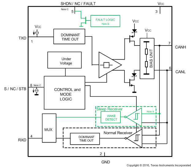
Functional Block Diagram

TCAN330 TCAN332 TCAN334 TCAN337 TCAN330G TCAN332G TCAN334G TCAN337G fbd_SLLSEQ7.gif
Sleep Receiver and Wake Detect are device dependent options and are only available in TCAND334.
Fault Logic is only available in TCAND337.
Pin 5 and 8 functions are device dependent. Refer to Device Options.