SLLSEZ5D January 2018 – June 2022 TCAN4550-Q1
PRODUCTION DATA
- 1 Features
- 2 Applications
- 3 Description
- 4 Revision History
- 5 Pin Configuration and Functions
-
6 Specification
- 6.1 Absolute Maximum Ratings
- 6.2 ESD Ratings
- 6.3 ESD Ratings, IEC ESD and ISO Transient Specification
- 6.4 Recommended Operating Conditions
- 6.5 Thermal Information
- 6.6 Supply Characteristics
- 6.7 Electrical Characteristics
- 6.8 Timing Requirements
- 6.9 Switching Characteristics
- 6.10 Typical Characteristics
- 7 Parameter Measurement Information
-
8 Detailed Description
- 8.1 Overview
- 8.2 Functional Block Diagram
- 8.3 Feature Description
- 8.4
Device Functional Modes
- 8.4.1 Normal Mode
- 8.4.2 Standby Mode
- 8.4.3 Sleep Mode
- 8.4.4 Test Mode
- 8.4.5 Failsafe Feature
- 8.4.6 Protection Features
- 8.4.7 CAN FD
- 8.5 Programming
- 8.6
Register Maps
- 8.6.1
Device ID and Interrupt/Diagnostic Flag Registers: 16'h0000 to 16'h002F
- 8.6.1.1 DEVICE_ID1[31:0] (address = h0000) [reset = h4E414354]
- 8.6.1.2 DEVICE_ID2[31:0] (address = h0004) [reset = h30353534]
- 8.6.1.3 Revision (address = h0008) [reset = h00110201]
- 8.6.1.4 Status (address = h000C) [reset = h0000000U]
- 8.6.1.5 SPI Error status mask (address = h0010) [reset = h00000000]
- 8.6.2 Device Configuration Registers: 16'h0800 to 16'h08FF
- 8.6.3 Interrupt/Diagnostic Flag and Enable Flag Registers: 16'h0820/0824 and 16'h0830
- 8.6.4
CAN FD Register Set: 16'h1000 to 16'h10FF
- 8.6.4.1 Core Release Register (address = h1000) [reset = hrrrddddd]
- 8.6.4.2 Endian Register (address = h1004) [reset = h87654321]
- 8.6.4.3 Customer Register (address = h1008) [reset = h00000000]
- 8.6.4.4 Data Bit Timing & Prescaler (address = h100C) [reset = h0000A33]
- 8.6.4.5 Test Register (address = h1010 ) [reset = h00000000]
- 8.6.4.6 RAM Watchdog (address = h1014) [reset = h00000000]
- 8.6.4.7 Control Register (address = h1018) [reset = 0000 0019]
- 8.6.4.8 Nominal Bit Timing & Prescaler Register (address = h101C) [reset = h06000A03]
- 8.6.4.9 Timestamp Counter Configuration (address = h1020) [reset = h00000000]
- 8.6.4.10 Timestamp Counter Value (address = h1024) [reset = h00000000]
- 8.6.4.11 Timeout Counter Configuration (address = h1028) [reset = hFFFF0000]
- 8.6.4.12 Timeout Counter Value (address = h102C) [reset = h0000FFFF]
- 8.6.4.13 Reserved (address = h1030 - h103C) [reset = h00000000]
- 8.6.4.14 Error Counter Register (address = h1040) [reset = h00000000]
- 8.6.4.15 Protocol Status Register (address = h1044) [reset = h00000707]
- 8.6.4.16 Transmitter Delay Compensation Register (address = h1048) [reset = h00000000]
- 8.6.4.17 Reserved (address = h104C) [reset = h00000000]
- 8.6.4.18 Interrupt Register (address = h1050) [reset = h00000000]
- 8.6.4.19 Interrupt Enable (address = h1054) [reset = h00000000]
- 8.6.4.20 Interrupt Line Select (address = h1058) [reset = h00000000]
- 8.6.4.21 Interrupt Line Enable (address = h105C) [reset = h00000000]
- 8.6.4.22 Reserved (address = h1060 - h107C) [reset = h00000000]
- 8.6.4.23 Global Filter Configuration (address = h1080) [reset = h00000000]
- 8.6.4.24 Standard ID Filter Configuration (address = h1084) [reset = h00000000]
- 8.6.4.25 Extended ID Filter Configuration (address = h1088) [reset = h00000000]
- 8.6.4.26 Reserved (address = h108C) [reset = h00000000]
- 8.6.4.27 Extended ID AND Mask (address = h1090) [reset = h1FFFFFFF]
- 8.6.4.28 High Priority Message Status (address = h1094) [reset = h00000000]
- 8.6.4.29 New Data 1 (address = h1098) [reset = h00000000]
- 8.6.4.30 New Data 2 (address = h109C) [reset = h00000000]
- 8.6.4.31 Rx FIFO 0 Configuration (address = h10A0) [reset = h00000000]
- 8.6.4.32 Rx FIFO 0 Status (address = h10A4) [reset = h00000000]
- 8.6.4.33 Rx FIFO 0 Acknowledge (address = h10A8) [reset = h00000000]
- 8.6.4.34 Rx Buffer Configuration (address = h10AC) [reset = h00000000]
- 8.6.4.35 Rx FIFO 1 Configuration (address = h10B0) [reset = h00000000]
- 8.6.4.36 Rx FIFO 1 Status (address = h10B4) [reset = h00000000]
- 8.6.4.37 Rx FIFO 1 Acknowledge (address = h10B8) [reset = h00000000]
- 8.6.4.38 Rx Buffer/FIFO Element Size Configuration (address = h10BC) [reset = h00000000]
- 8.6.4.39 Tx Buffer Configuration (address = h10C0) [reset = h00000000]
- 8.6.4.40 Tx FIFO/Queue Status (address = h10C4) [reset = h00000000]
- 8.6.4.41 Tx Buffer Element Size Configuration (address = h10C8) [reset = h00000000]
- 8.6.4.42 Tx Buffer Request Pending (address = h10CC) [reset = h00000000]
- 8.6.4.43
Tx Buffer Add Request (address = h10D0) [reset = h00000000]
- 8.6.4.43.1 Tx Buffer Cancellation Request (address = h10D4 [reset = h00000000]
- 8.6.4.43.2 Tx Buffer Add Request Transmission Occurred (address = h10D8) [reset = h00000000]
- 8.6.4.43.3 Tx Buffer Cancellation Finished (address = h10DC) [reset = h00000000]
- 8.6.4.43.4 Tx Buffer Transmission Interrupt Enable (address = h10E0) [reset = h00000000]
- 8.6.4.43.5 Tx Buffer Cancellation Finished Interrupt Enable (address = h10E4) [reset = h00000000]
- 8.6.4.43.6 Reserved (address = h10E8) [reset = h00000000]
- 8.6.4.43.7 Reserved (address = h10EC) [reset = h00000000]
- 8.6.4.43.8 Tx Event FIFO Configuration (address = h10F0) [reset = h00000000]
- 8.6.4.43.9 Tx Event FIFO Status (address = h10F4) [reset = h00000000]
- 8.6.4.43.10 Tx Event FIFO Acknowledge (address = h10F8) [reset = h00000000]
- 8.6.4.43.11 Reserved (address = h10FC) [reset = h00000000]
- 8.6.1
Device ID and Interrupt/Diagnostic Flag Registers: 16'h0000 to 16'h002F
- 9 Application and Implementation
- 10Power Supply Recommendations
- 11Layout
- 12Device and Documentation Support
- 13Mechanical, Packaging, and Orderable Information
Package Options
Mechanical Data (Package|Pins)
- RGY|20
Thermal pad, mechanical data (Package|Pins)
- RGY|20
Orderable Information
9.2.3 Application Curves
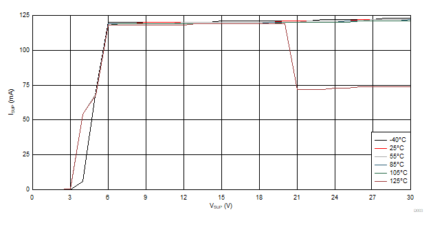
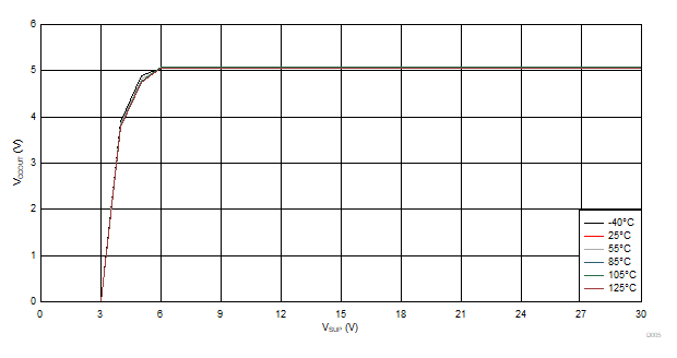
Figure 9-8 and Figure 9-9 shows the behavior of the 5 V LDO in relationship to ISUP, VSUP, LDO load of 70 mA, CAN bus dominant and ambient temperature. The ISUP current is based upon a 70 mA load on VCCOUT and the CAN bus held dominant for about a total of 120 mA. As can be seen, an ambient temperature of 125°C can cause a thermal shut down event when VSUP reaches 20 V and VCCOUT is providing 70 mA to a load. The load on the CAN bus is 60 Ω. When the CAN bus load is 50 Ω a VSUP of 19 V and ambient temperature of 125 can trigger a thermal shut down event. The reason the curve shows ISUP leveling out to approximately 74.5 mA is due to thermal shut down where the device shuts off the LDO and CAN transceiver. The device cools below TSD leaving thermal shutdown quickly. When the TSD event goes away the device then enters standby mode, turning on the LDO. The 74.5 mA is the 70 mA LDO load and a dominant on the CAN bus in standby mode. This is happening quickly enough that LDO shut off is not seen. If the TSD event is prolonged the current would drop to micro-amps and VCCOUT would be 0 V once the decoupling capacitor discharges.

| VCCOUT = 5 V at 70 mA | CAN Bus = Dominant | CAN Load = 60 Ω |

| VCCOUT = 5 V at 70 mA | CAN Bus = Dominant | CAN Load = 60 Ω |