SLLSEZ5D January 2018 – June 2022 TCAN4550-Q1
PRODUCTION DATA
- 1 Features
- 2 Applications
- 3 Description
- 4 Revision History
- 5 Pin Configuration and Functions
-
6 Specification
- 6.1 Absolute Maximum Ratings
- 6.2 ESD Ratings
- 6.3 ESD Ratings, IEC ESD and ISO Transient Specification
- 6.4 Recommended Operating Conditions
- 6.5 Thermal Information
- 6.6 Supply Characteristics
- 6.7 Electrical Characteristics
- 6.8 Timing Requirements
- 6.9 Switching Characteristics
- 6.10 Typical Characteristics
- 7 Parameter Measurement Information
-
8 Detailed Description
- 8.1 Overview
- 8.2 Functional Block Diagram
- 8.3 Feature Description
- 8.4
Device Functional Modes
- 8.4.1 Normal Mode
- 8.4.2 Standby Mode
- 8.4.3 Sleep Mode
- 8.4.4 Test Mode
- 8.4.5 Failsafe Feature
- 8.4.6 Protection Features
- 8.4.7 CAN FD
- 8.5 Programming
- 8.6
Register Maps
- 8.6.1
Device ID and Interrupt/Diagnostic Flag Registers: 16'h0000 to 16'h002F
- 8.6.1.1 DEVICE_ID1[31:0] (address = h0000) [reset = h4E414354]
- 8.6.1.2 DEVICE_ID2[31:0] (address = h0004) [reset = h30353534]
- 8.6.1.3 Revision (address = h0008) [reset = h00110201]
- 8.6.1.4 Status (address = h000C) [reset = h0000000U]
- 8.6.1.5 SPI Error status mask (address = h0010) [reset = h00000000]
- 8.6.2 Device Configuration Registers: 16'h0800 to 16'h08FF
- 8.6.3 Interrupt/Diagnostic Flag and Enable Flag Registers: 16'h0820/0824 and 16'h0830
- 8.6.4
CAN FD Register Set: 16'h1000 to 16'h10FF
- 8.6.4.1 Core Release Register (address = h1000) [reset = hrrrddddd]
- 8.6.4.2 Endian Register (address = h1004) [reset = h87654321]
- 8.6.4.3 Customer Register (address = h1008) [reset = h00000000]
- 8.6.4.4 Data Bit Timing & Prescaler (address = h100C) [reset = h0000A33]
- 8.6.4.5 Test Register (address = h1010 ) [reset = h00000000]
- 8.6.4.6 RAM Watchdog (address = h1014) [reset = h00000000]
- 8.6.4.7 Control Register (address = h1018) [reset = 0000 0019]
- 8.6.4.8 Nominal Bit Timing & Prescaler Register (address = h101C) [reset = h06000A03]
- 8.6.4.9 Timestamp Counter Configuration (address = h1020) [reset = h00000000]
- 8.6.4.10 Timestamp Counter Value (address = h1024) [reset = h00000000]
- 8.6.4.11 Timeout Counter Configuration (address = h1028) [reset = hFFFF0000]
- 8.6.4.12 Timeout Counter Value (address = h102C) [reset = h0000FFFF]
- 8.6.4.13 Reserved (address = h1030 - h103C) [reset = h00000000]
- 8.6.4.14 Error Counter Register (address = h1040) [reset = h00000000]
- 8.6.4.15 Protocol Status Register (address = h1044) [reset = h00000707]
- 8.6.4.16 Transmitter Delay Compensation Register (address = h1048) [reset = h00000000]
- 8.6.4.17 Reserved (address = h104C) [reset = h00000000]
- 8.6.4.18 Interrupt Register (address = h1050) [reset = h00000000]
- 8.6.4.19 Interrupt Enable (address = h1054) [reset = h00000000]
- 8.6.4.20 Interrupt Line Select (address = h1058) [reset = h00000000]
- 8.6.4.21 Interrupt Line Enable (address = h105C) [reset = h00000000]
- 8.6.4.22 Reserved (address = h1060 - h107C) [reset = h00000000]
- 8.6.4.23 Global Filter Configuration (address = h1080) [reset = h00000000]
- 8.6.4.24 Standard ID Filter Configuration (address = h1084) [reset = h00000000]
- 8.6.4.25 Extended ID Filter Configuration (address = h1088) [reset = h00000000]
- 8.6.4.26 Reserved (address = h108C) [reset = h00000000]
- 8.6.4.27 Extended ID AND Mask (address = h1090) [reset = h1FFFFFFF]
- 8.6.4.28 High Priority Message Status (address = h1094) [reset = h00000000]
- 8.6.4.29 New Data 1 (address = h1098) [reset = h00000000]
- 8.6.4.30 New Data 2 (address = h109C) [reset = h00000000]
- 8.6.4.31 Rx FIFO 0 Configuration (address = h10A0) [reset = h00000000]
- 8.6.4.32 Rx FIFO 0 Status (address = h10A4) [reset = h00000000]
- 8.6.4.33 Rx FIFO 0 Acknowledge (address = h10A8) [reset = h00000000]
- 8.6.4.34 Rx Buffer Configuration (address = h10AC) [reset = h00000000]
- 8.6.4.35 Rx FIFO 1 Configuration (address = h10B0) [reset = h00000000]
- 8.6.4.36 Rx FIFO 1 Status (address = h10B4) [reset = h00000000]
- 8.6.4.37 Rx FIFO 1 Acknowledge (address = h10B8) [reset = h00000000]
- 8.6.4.38 Rx Buffer/FIFO Element Size Configuration (address = h10BC) [reset = h00000000]
- 8.6.4.39 Tx Buffer Configuration (address = h10C0) [reset = h00000000]
- 8.6.4.40 Tx FIFO/Queue Status (address = h10C4) [reset = h00000000]
- 8.6.4.41 Tx Buffer Element Size Configuration (address = h10C8) [reset = h00000000]
- 8.6.4.42 Tx Buffer Request Pending (address = h10CC) [reset = h00000000]
- 8.6.4.43
Tx Buffer Add Request (address = h10D0) [reset = h00000000]
- 8.6.4.43.1 Tx Buffer Cancellation Request (address = h10D4 [reset = h00000000]
- 8.6.4.43.2 Tx Buffer Add Request Transmission Occurred (address = h10D8) [reset = h00000000]
- 8.6.4.43.3 Tx Buffer Cancellation Finished (address = h10DC) [reset = h00000000]
- 8.6.4.43.4 Tx Buffer Transmission Interrupt Enable (address = h10E0) [reset = h00000000]
- 8.6.4.43.5 Tx Buffer Cancellation Finished Interrupt Enable (address = h10E4) [reset = h00000000]
- 8.6.4.43.6 Reserved (address = h10E8) [reset = h00000000]
- 8.6.4.43.7 Reserved (address = h10EC) [reset = h00000000]
- 8.6.4.43.8 Tx Event FIFO Configuration (address = h10F0) [reset = h00000000]
- 8.6.4.43.9 Tx Event FIFO Status (address = h10F4) [reset = h00000000]
- 8.6.4.43.10 Tx Event FIFO Acknowledge (address = h10F8) [reset = h00000000]
- 8.6.4.43.11 Reserved (address = h10FC) [reset = h00000000]
- 8.6.1
Device ID and Interrupt/Diagnostic Flag Registers: 16'h0000 to 16'h002F
- 9 Application and Implementation
- 10Power Supply Recommendations
- 11Layout
- 12Device and Documentation Support
- 13Mechanical, Packaging, and Orderable Information
Package Options
Mechanical Data (Package|Pins)
- RGY|20
Thermal pad, mechanical data (Package|Pins)
- RGY|20
Orderable Information
8.4.3.1 Bus Wake via RXD_INT Request (BWRR) in Sleep Mode
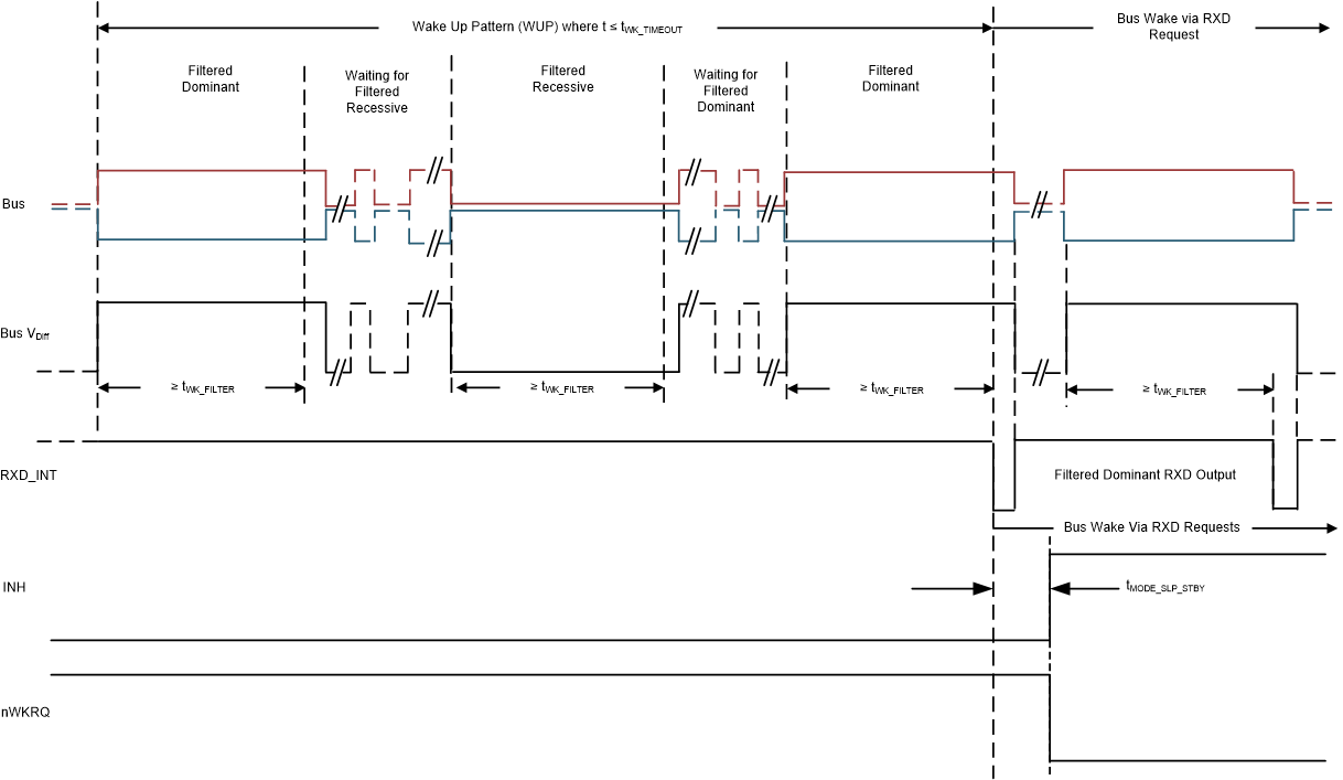
The TCAN4550-Q1 supports low power sleep mode, and uses a wake-up from the CAN bus mechanism called bus wake via RXD_INT Request (BWRR). Once this pattern is received, the TCAN4550-Q1 automatically switches to standby mode and inserts an interrupt onto the nINT and nWKRQ pins to indicate to a host microprocessor that the bus is active, and it should wake-up and service the TCAN4550-Q1. The low power receiver and bus monitor are enabled in sleep mode to allow for RXD_INT Wake Requests via the CAN bus. A wake-up request is output to the internal RXD_INT (driven low) as shown in Figure 8-7. The wake logic monitors RXD_INT for transitions (high to low) and reactivate the device to standby mode based on the RXD_INT Wake Request. The CAN bus terminals are weakly pulled to GND during this mode, see Figure 7-2.
These devices use the wake-up pattern (WUP) from ISO 11898-2:2016 to qualify bus traffic into a request to wake the host microprocessor. The bus wake request is signaled to the integrated CAN FD controller by a falling edge and low corresponding to a “filtered” bus dominant on the RXD_INT terminal (BWRR).
The wake-up pattern (WUP) consists of
- A filtered dominant bus of at least tWK_FILTER followed by
- A filtered recessive bus time of at least tWK_FILTER followed by
- A second filtered dominant bus time of at least tWK_FILTER
Once the WUP is detected, the device starts issuing wake-up requests (BWRR) on the RXD_INT signal every time a filtered dominant time is received from the bus. The first filtered dominant initiates the WUP and the bus monitor is now waiting on a filtered recessive, other bus traffic does not reset the bus monitor. Once a filtered recessive is received, the bus monitor is now waiting on a filtered dominant and again, other bus traffic does not reset the bus monitor. Immediately upon receiving the second filtered dominant and verification of receiving a WUP, the device transitions the bus monitor into BWRR mode. This indicates all filtered dominant bus times on the RXD_INT internal signal by driving it low for the dominant bus time that is in excess of tWK_FILTER. The RXD_INT output during BWRR matches the classical 8-pin CAN devices that used the single, filtered dominant on the bus as the wake-up request mechanism from ISO 11898-2:2016.
For a dominant or recessive to be considered “filtered”, the bus must be in that state for more than tWK_FILTER time. Due to variability in the tWK_FILTER the following scenarios are applicable.
- Bus state times less than tWK_FILTER(MIN) are never detected as part of a WUP, and thus no BWRR is generated.
- Bus state times between tWK_FILTER(MIN) and tWK_FILTER(MAX) may be detected as part of a WUP and a BWRR may be generated.
- Bus state times more than tWK_FILTER(MAX) is always detected as part of a WUP, and thus, a BWRR is always be generated.
See Figure 8-6 for the timing diagram of the WUP.
The pattern and tWK_FILTER time used for the WUP and BWRR prevents noise and bus stuck dominant faults from causing false wake requests while allowing any CAN or CAN FD message to initiate a BWRR. If the device is switched to normal mode or an under-voltage event occurs on VCC, the BWRR is lost. The WUP pattern must take place within the tWK_TIMEOUT time; otherwise. the device is in a state waiting for the next recessive and then a valid WUP pattern.
 Figure 8-6 Wake-Up Pattern (WUP) and Bus Wake via RXD_INT Request (BWRR)
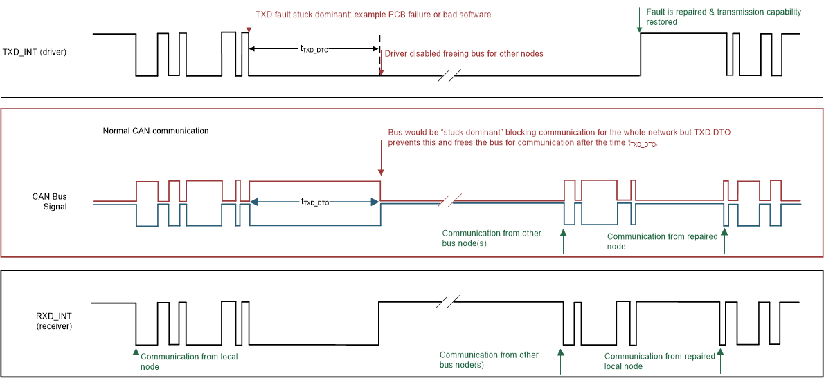
 Figure 8-7 Example timing diagram with TXD_INT DTO