SLLSEZ5D January 2018 – June 2022 TCAN4550-Q1
PRODUCTION DATA
- 1 Features
- 2 Applications
- 3 Description
- 4 Revision History
- 5 Pin Configuration and Functions
-
6 Specification
- 6.1 Absolute Maximum Ratings
- 6.2 ESD Ratings
- 6.3 ESD Ratings, IEC ESD and ISO Transient Specification
- 6.4 Recommended Operating Conditions
- 6.5 Thermal Information
- 6.6 Supply Characteristics
- 6.7 Electrical Characteristics
- 6.8 Timing Requirements
- 6.9 Switching Characteristics
- 6.10 Typical Characteristics
- 7 Parameter Measurement Information
-
8 Detailed Description
- 8.1 Overview
- 8.2 Functional Block Diagram
- 8.3 Feature Description
- 8.4
Device Functional Modes
- 8.4.1 Normal Mode
- 8.4.2 Standby Mode
- 8.4.3 Sleep Mode
- 8.4.4 Test Mode
- 8.4.5 Failsafe Feature
- 8.4.6 Protection Features
- 8.4.7 CAN FD
- 8.5 Programming
- 8.6
Register Maps
- 8.6.1
Device ID and Interrupt/Diagnostic Flag Registers: 16'h0000 to 16'h002F
- 8.6.1.1 DEVICE_ID1[31:0] (address = h0000) [reset = h4E414354]
- 8.6.1.2 DEVICE_ID2[31:0] (address = h0004) [reset = h30353534]
- 8.6.1.3 Revision (address = h0008) [reset = h00110201]
- 8.6.1.4 Status (address = h000C) [reset = h0000000U]
- 8.6.1.5 SPI Error status mask (address = h0010) [reset = h00000000]
- 8.6.2 Device Configuration Registers: 16'h0800 to 16'h08FF
- 8.6.3 Interrupt/Diagnostic Flag and Enable Flag Registers: 16'h0820/0824 and 16'h0830
- 8.6.4
CAN FD Register Set: 16'h1000 to 16'h10FF
- 8.6.4.1 Core Release Register (address = h1000) [reset = hrrrddddd]
- 8.6.4.2 Endian Register (address = h1004) [reset = h87654321]
- 8.6.4.3 Customer Register (address = h1008) [reset = h00000000]
- 8.6.4.4 Data Bit Timing & Prescaler (address = h100C) [reset = h0000A33]
- 8.6.4.5 Test Register (address = h1010 ) [reset = h00000000]
- 8.6.4.6 RAM Watchdog (address = h1014) [reset = h00000000]
- 8.6.4.7 Control Register (address = h1018) [reset = 0000 0019]
- 8.6.4.8 Nominal Bit Timing & Prescaler Register (address = h101C) [reset = h06000A03]
- 8.6.4.9 Timestamp Counter Configuration (address = h1020) [reset = h00000000]
- 8.6.4.10 Timestamp Counter Value (address = h1024) [reset = h00000000]
- 8.6.4.11 Timeout Counter Configuration (address = h1028) [reset = hFFFF0000]
- 8.6.4.12 Timeout Counter Value (address = h102C) [reset = h0000FFFF]
- 8.6.4.13 Reserved (address = h1030 - h103C) [reset = h00000000]
- 8.6.4.14 Error Counter Register (address = h1040) [reset = h00000000]
- 8.6.4.15 Protocol Status Register (address = h1044) [reset = h00000707]
- 8.6.4.16 Transmitter Delay Compensation Register (address = h1048) [reset = h00000000]
- 8.6.4.17 Reserved (address = h104C) [reset = h00000000]
- 8.6.4.18 Interrupt Register (address = h1050) [reset = h00000000]
- 8.6.4.19 Interrupt Enable (address = h1054) [reset = h00000000]
- 8.6.4.20 Interrupt Line Select (address = h1058) [reset = h00000000]
- 8.6.4.21 Interrupt Line Enable (address = h105C) [reset = h00000000]
- 8.6.4.22 Reserved (address = h1060 - h107C) [reset = h00000000]
- 8.6.4.23 Global Filter Configuration (address = h1080) [reset = h00000000]
- 8.6.4.24 Standard ID Filter Configuration (address = h1084) [reset = h00000000]
- 8.6.4.25 Extended ID Filter Configuration (address = h1088) [reset = h00000000]
- 8.6.4.26 Reserved (address = h108C) [reset = h00000000]
- 8.6.4.27 Extended ID AND Mask (address = h1090) [reset = h1FFFFFFF]
- 8.6.4.28 High Priority Message Status (address = h1094) [reset = h00000000]
- 8.6.4.29 New Data 1 (address = h1098) [reset = h00000000]
- 8.6.4.30 New Data 2 (address = h109C) [reset = h00000000]
- 8.6.4.31 Rx FIFO 0 Configuration (address = h10A0) [reset = h00000000]
- 8.6.4.32 Rx FIFO 0 Status (address = h10A4) [reset = h00000000]
- 8.6.4.33 Rx FIFO 0 Acknowledge (address = h10A8) [reset = h00000000]
- 8.6.4.34 Rx Buffer Configuration (address = h10AC) [reset = h00000000]
- 8.6.4.35 Rx FIFO 1 Configuration (address = h10B0) [reset = h00000000]
- 8.6.4.36 Rx FIFO 1 Status (address = h10B4) [reset = h00000000]
- 8.6.4.37 Rx FIFO 1 Acknowledge (address = h10B8) [reset = h00000000]
- 8.6.4.38 Rx Buffer/FIFO Element Size Configuration (address = h10BC) [reset = h00000000]
- 8.6.4.39 Tx Buffer Configuration (address = h10C0) [reset = h00000000]
- 8.6.4.40 Tx FIFO/Queue Status (address = h10C4) [reset = h00000000]
- 8.6.4.41 Tx Buffer Element Size Configuration (address = h10C8) [reset = h00000000]
- 8.6.4.42 Tx Buffer Request Pending (address = h10CC) [reset = h00000000]
- 8.6.4.43
Tx Buffer Add Request (address = h10D0) [reset = h00000000]
- 8.6.4.43.1 Tx Buffer Cancellation Request (address = h10D4 [reset = h00000000]
- 8.6.4.43.2 Tx Buffer Add Request Transmission Occurred (address = h10D8) [reset = h00000000]
- 8.6.4.43.3 Tx Buffer Cancellation Finished (address = h10DC) [reset = h00000000]
- 8.6.4.43.4 Tx Buffer Transmission Interrupt Enable (address = h10E0) [reset = h00000000]
- 8.6.4.43.5 Tx Buffer Cancellation Finished Interrupt Enable (address = h10E4) [reset = h00000000]
- 8.6.4.43.6 Reserved (address = h10E8) [reset = h00000000]
- 8.6.4.43.7 Reserved (address = h10EC) [reset = h00000000]
- 8.6.4.43.8 Tx Event FIFO Configuration (address = h10F0) [reset = h00000000]
- 8.6.4.43.9 Tx Event FIFO Status (address = h10F4) [reset = h00000000]
- 8.6.4.43.10 Tx Event FIFO Acknowledge (address = h10F8) [reset = h00000000]
- 8.6.4.43.11 Reserved (address = h10FC) [reset = h00000000]
- 8.6.1
Device ID and Interrupt/Diagnostic Flag Registers: 16'h0000 to 16'h002F
- 9 Application and Implementation
- 10Power Supply Recommendations
- 11Layout
- 12Device and Documentation Support
- 13Mechanical, Packaging, and Orderable Information
Package Options
Mechanical Data (Package|Pins)
- RGY|20
Thermal pad, mechanical data (Package|Pins)
- RGY|20
Orderable Information
8.3.8 RST Pin
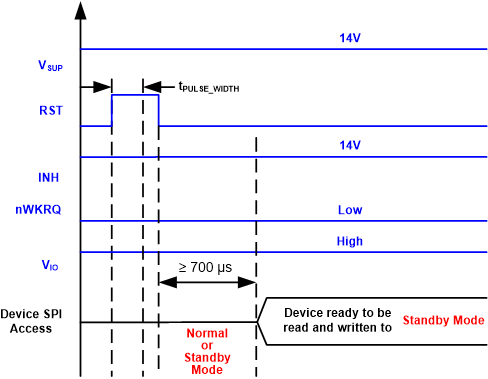
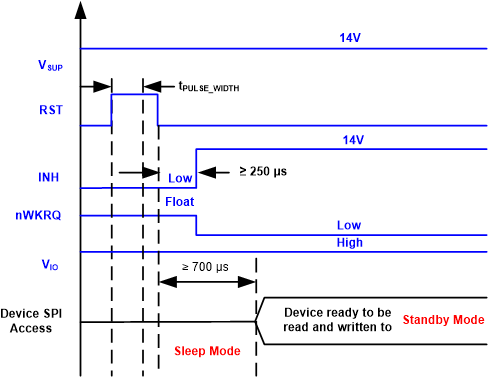
The RST pin is a device reset pin. It has a weak internal pull-down resistor for normal operation. If communication has stopped with the TCAN4550-Q1, the RST pin can be pulsed high and then back low for greater than tPULSE_WIDTH to perform a power on reset to the device. This resets the device to the default settings and puts the device into standby mode. If the device was in normal or standby mode the INH and nWKRQ pins remain active (on) and do not toggle; see Figure 8-3. If the device is in sleep mode and reset is toggled the device enters standby mode and at that time INH and nWKRQ turns on; see Figure 8-4.
After a RST has taken place, a wait time of ≥ 700 µs should be used before reading or writing to the TCAN4550-Q1.
 Figure 8-3 Timing for RST Pin in Normal and Standby Modes
 Figure 8-4 Timing for RST Pin in Sleep Mode