SLLSEX2F December 2016 – April 2024 TDP158
PRODUCTION DATA
- 1
- 1 Features
- 2 Applications
- 3 Description
- 4 Pin Configuration and Functions
-
5 Specifications
- 5.1 Absolute Maximum Ratings
- 5.2 ESD Ratings
- 5.3 Recommended Operating Conditions
- 5.4 Thermal Information
- 5.5 Electrical Characteristics, Power Supply
- 5.6 Electrical Characteristics, Differential Input
- 5.7 Electrical Characteristics, TMDS Differential Output
- 5.8 Electrical Characteristics, DDC, I2C, HPD, and ARC
- 5.9 Electrical Characteristics, TMDS Differential Output in DP-Mode
- 5.10 Switching Characteristics, TMDS
- 5.11 Switching Characteristics, HPD
- 5.12 Switching Characteristics, DDC and I2C
- 5.13 Typical Characteristics
- 6 Parameter Measurement Information
-
7 Detailed Description
- 7.1 Overview
- 7.2 Functional Block Diagram
- 7.3 Feature Description
- 7.4 Device Functional Modes
- 7.5
Register Maps
- 7.5.1 Local I2C Control BIT Access TAG Convention
- 7.5.2 BIT Access Tag Conventions
- 7.5.3 CSR Bit Field Definitions, DEVICE_ID (address = 00h≅07h)
- 7.5.4 CSR Bit Field Definitions, REV_ID (address = 08h )
- 7.5.5 CSR Bit Field Definitions – MISC CONTROL 09h (address = 09h)
- 7.5.6 CSR Bit Field Definitions – MISC CONTROL 0Ah (address = 0Ah)
- 7.5.7 CSR Bit Field Definitions – MISC CONTROL 0Bh (address = 0Bh)
- 7.5.8 CSR Bit Field Definitions – MISC CONTROL 0Ch (address = 0Ch)
- 7.5.9 CSR Bit Field Definitions, Equalization Control Register (address = 0Dh)
- 7.5.10 CSR Bit Field Definitions, POWER MODE STATUS (address = 20h)
- 7.5.11 CSR Bit Field Definitions, DP-Mode and INDIVIDUAL LANE CONTROL (address = 30h)
- 7.5.12 CSR Bit Field Definitions, DP-Mode and INDIVIDUAL LANE CONTROL (address = 31h)
- 7.5.13 CSR Bit Field Definitions, DP-Mode and INDIVIDUAL LANE CONTROL (address = 32h)
- 7.5.14 CSR Bit Field Definitions, DP-Mode and INDIVIDUAL LANE CONTROL (address = 33h)
- 7.5.15 CSR Bit Field Definitions, DP-Mode and INDIVIDUAL LANE CONTROL (address = 34h)
- 7.5.16 CSR Bit Field Definitions, DP-Mode and INDIVIDUAL LANE CONTROL (address = 35h)
- 7.5.17 CSR Bit Field Definitions, DP-Mode and INDIVIDUAL LANE CONTROL (address = 4Dh)
- 7.5.18 CSR Bit Field Definitions, DP-Mode and INDIVIDUAL LANE CONTROL (address = 4Eh)
- 7.5.19 CSR Bit Field Definitions, DP-Mode and INDIVIDUAL LANE CONTROL (address = 4Fh)
- 8 Application and Implementation
- 9 Device and Documentation Support
- 10Revision History
- 11Mechanical, Packaging, and Orderable Information
Package Options
Mechanical Data (Package|Pins)
- RSB|40
Thermal pad, mechanical data (Package|Pins)
- RSB|40
Orderable Information
3 Description
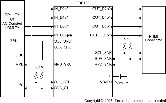
The TDP158 device is an AC-coupled HDMI signal to transition-minimized differential signal (TMDS) Redriver supporting digital video interface (DVI) 1.0 and high-definition multimedia interface (HDMI) 1.4b and 2.0b output signals. The TDP158 supports four TMDS channels and Digital Display Control (DDC) interfaces. The TDP158 supports signaling rates up to 6Gbps to allow for the highest resolutions of 4k 2k 60p 24 bits per pixel and up to WUXGA 16-bit color depth or 1080p with higher refresh rates. The TDP158 can be configured to support the HDMI 2.0 standard.
The TDP158 supports dual power supply
rails of
1.1V on VDD and 3.3V on
VCC for power reduction. Several methods of power management are
implemented to reduce overall power consumption. TDP158 supports fixed receiver EQ
gain using I2C or pin strap to compensate for different lengths input
cable or board traces.
 Simplified Schematic
 Display