SBOS875C August 2017 – February 2023 THS3491
PRODUCTION DATA
- 1 Features
- 2 Applications
- 3 Description
- 4 Revision History
- 5 Device Comparison Table
- 6 Pin Configuration and Functions
- 7 Bare Die Information
- 8 Specifications
- 9 Detailed Description
- 10Application and Implementation
- 11Device and Documentation Support
- 12Mechanical, Packaging, and Orderable Information
Package Options
Mechanical Data (Package|Pins)
Thermal pad, mechanical data (Package|Pins)
Orderable Information
10.4.1.1.2 Power Dissipation and Thermal Considerations
The THS3491 includes automatic thermal shutoff protection. This protection circuitry shuts down the amplifier if the junction temperature exceeds approximately 160°C. When the junction temperature decreases to approximately 145°C, the amplifier turns on again. However, for maximum performance and reliability, make sure that the design does not exceed a junction temperature of 125°C. Between 125°C and 150°C, damage does not occur, but the performance of the amplifier begins to degrade and long-term reliability suffers. The package and the PCB dictate the thermal characteristics of the device. Maximum power dissipation for a particular package is calculated using the following formula.
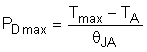
where
- PDmax is the maximum power dissipation in the amplifier (W).
- Tmax is the absolute maximum junction temperature (°C).
- TA is the ambient temperature (°C).
- θJA = θJC + θCA
- θJC is the thermal coefficient from the silicon junctions to the case (°C/W).
- θCA is the thermal coefficient from the case to ambient air (°C/W).
The thermal coefficient for the PowerPAD integrated circuit packages are substantially improved over the traditional SOIC package. The data for the PowerPAD packages assume a board layout that follows the PowerPAD package layout guidelines referenced above and detailed in PowerPAD™ Thermally Enhanced Package. Maximum power dissipation levels are shown in Comparison of θJA for Various Packages. If the PowerPAD integrated circuit package is not soldered to the PCB, the thermal impedance increases substantially and may cause serious heat and performance issues. Take care to always solder the PowerPAD integrated circuit package to the PCB for optimum performance.
When determining whether or not the device satisfies the maximum power dissipation requirement, make sure to consider not only quiescent power dissipation, but dynamic power dissipation. Often times, this dissipation is difficult to quantify because the signal pattern is inconsistent, but an estimate of the RMS power dissipation provides visibility into a possible problem.