SLOS823D December 2012 – March 2020 THS4531A
PRODUCTION DATA.
- 1 Features
- 2 Applications
- 3 Description
- 4 Revision History
- 5 Related Products
- 6 Pin Configuration and Functions
- 7 Specifications
- 8 Detailed Description
-
9 Application and Implementation
- 9.1
Application Information
- 9.1.1 Frequency Response, and Output Impedance
- 9.1.2 Distortion
- 9.1.3 Slew Rate, Transient Response, Settling Time, Overdrive, Output Voltage, and Turnon and Turnoff Time
- 9.1.4 Common-Mode and Power Supply Rejection
- 9.1.5 VOCM Input
- 9.1.6 Balance Error
- 9.1.7 Single-Supply Operation
- 9.1.8 Low-Power Applications and the Effects of Resistor Values on Bandwidth
- 9.1.9 Driving Capacitive Loads
- 9.1.10 Audio Performance
- 9.1.11 Audio On and Off Pop Performance
- 9.2
Typical Applications
- 9.2.1 SAR ADC Performance: THS4531A and ADS8321 Combined Performance
- 9.2.2 Audio ADC Driver Performance: THS4531A and PCM4204 Combined Performance
- 9.2.3 SAR ADC Performance: THS4531A and ADS7945 Combined Performance
- 9.2.4 Differential-Input to Differential-Output Amplifier
- 9.2.5 Single-Ended to Differential FDA Configuration
- 9.2.6 Single-Ended Input to Differential Output Amplifier
- 9.2.7 Differential Input to Single-Ended Output Amplifier
- 9.1
Application Information
- 10Power Supply Recommendations
- 11Layout
- 12Device and Documentation Support
- 13Mechanical, Packaging, and Orderable Information
Package Options
Mechanical Data (Package|Pins)
Thermal pad, mechanical data (Package|Pins)
Orderable Information
9.2.4.1 AC-Coupled, Differential-Input to Differential-Output Design Issues
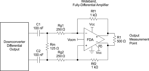
There are two typical ways to use the THS4531A family with an AC-coupled differential source. In the first method, the source is differential and can be coupled in through two blocking capacitors. The second method uses either a single-ended or a differential source and couples in through a transformer (or balun). Figure 93 shows a typical blocking capacitor approach to a differential input. An optional differential-input termination resistor (RM) is included in this design. This RM element allows the input RG resistors to be scaled up while still delivering lower differential input impedance to the source. In this example, the RG elements sum to show a 500-Ω differential impedance, while the RM element combines in parallel to give a net 100-Ω, AC-coupled, differential impedance to the source. Again, the design proceeds ideally by selecting the RF element values, then the RG to set the differential gain, then an RM element (if needed) to achieve the target input impedance. Alternatively, the RM element can be eliminated, the RG elements set to the desired input impedance, and RF set to the get the differential gain (RF / RG).
 Figure 93. Example Down-Converting Mixer Delivering an AC-Coupled Differential Signal to the THS4531A
 The DC biasing here is very simple. The output VOCM is set by the input control voltage; and because there is no DC-current path for the output common-mode voltage, that DC bias also sets the input pins common-mode operating points.