SLOS823D December 2012 – March 2020 THS4531A
PRODUCTION DATA.
- 1 Features
- 2 Applications
- 3 Description
- 4 Revision History
- 5 Related Products
- 6 Pin Configuration and Functions
- 7 Specifications
- 8 Detailed Description
-
9 Application and Implementation
- 9.1
Application Information
- 9.1.1 Frequency Response, and Output Impedance
- 9.1.2 Distortion
- 9.1.3 Slew Rate, Transient Response, Settling Time, Overdrive, Output Voltage, and Turnon and Turnoff Time
- 9.1.4 Common-Mode and Power Supply Rejection
- 9.1.5 VOCM Input
- 9.1.6 Balance Error
- 9.1.7 Single-Supply Operation
- 9.1.8 Low-Power Applications and the Effects of Resistor Values on Bandwidth
- 9.1.9 Driving Capacitive Loads
- 9.1.10 Audio Performance
- 9.1.11 Audio On and Off Pop Performance
- 9.2
Typical Applications
- 9.2.1 SAR ADC Performance: THS4531A and ADS8321 Combined Performance
- 9.2.2 Audio ADC Driver Performance: THS4531A and PCM4204 Combined Performance
- 9.2.3 SAR ADC Performance: THS4531A and ADS7945 Combined Performance
- 9.2.4 Differential-Input to Differential-Output Amplifier
- 9.2.5 Single-Ended to Differential FDA Configuration
- 9.2.6 Single-Ended Input to Differential Output Amplifier
- 9.2.7 Differential Input to Single-Ended Output Amplifier
- 9.1
Application Information
- 10Power Supply Recommendations
- 11Layout
- 12Device and Documentation Support
- 13Mechanical, Packaging, and Orderable Information
Package Options
Mechanical Data (Package|Pins)
Thermal pad, mechanical data (Package|Pins)
Orderable Information
9.2.6.1 AC-Coupled Signal Path Considerations for Single-Ended Input to Differential Output Conversion
When the signal path can be AC-coupled, the DC biasing for the THS4531A family becomes a relatively simple task. In all designs, start by defining the output common-mode voltage. The AC-coupling issue can be separated for the input and output sides of an FDA design. The input can be AC-coupled and the output DC-coupled, or the output can be ac-coupled and the input dc-coupled, or they can both be AC-coupled.
One situation where the output might be DC-coupled (for an AC-coupled input), is when driving directly into an ADC where the VOCM control voltage uses the ADC common-mode reference to directly bias the FDA output common-mode to the required ADC input common-mode. In any case, the design starts by setting the desired VOCM.
When an AC-coupled path follows the output pins, the best linearity is achieved by operating VOCM at midsupply. The VOCM voltage must be within the linear range for the common-mode loop, as specified in the headroom specifications (approximately 0.91 V greater than the negative supply and 1.1 V less than the positive supply). If the output path is also ac-coupled, simply letting the VOCM control pin float is usually preferred to get a midsupply default VOCM bias with minimal elements. To limit noise, place a 0.1-µF decoupling capacitor on the VOCM pin to ground.
After VOCM is defined, check the target output voltage swing to ensure that the VOCM plus the positive and negative output swing on each side do not clip into the supplies. If the desired output differential swing is defined as VOPP, divide by 4 to obtain the ±VP swing around VOCM at each of the two output pins (each pin operates 180° out of phase with the other). Check that VOCM ±VP does not exceed the absolute supply rails for this rail-to-rail output (RRO) device.
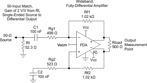
Going to the device input pins side, because both the source and balancing resistor on the nonsignal input side are DC-blocked (see Figure 96), no common-mode current flows from the output common-mode voltage, thus setting the input common-mode equal to the output common-mode voltage.
This input headroom also sets a limit for higher VOCM voltages. Because the input VICM is the output VOCM for ac-coupled sources, the 1.2-V minimum headroom for the input pins to the positive supply overrides the 1.1-V headroom limit for the output VOCM. Also, the input signal moves this input VICM around the dc bias point, as described in the section Resistor Design Equations for the Single-Ended to Differential Configuration of the FDA.
 Figure 96. AC-Coupled, Single-Ended Source to a Differential Gain of 2 V/V Test Circuit