SLOS823D December 2012 – March 2020 THS4531A
PRODUCTION DATA.
- 1 Features
- 2 Applications
- 3 Description
- 4 Revision History
- 5 Related Products
- 6 Pin Configuration and Functions
- 7 Specifications
- 8 Detailed Description
-
9 Application and Implementation
- 9.1
Application Information
- 9.1.1 Frequency Response, and Output Impedance
- 9.1.2 Distortion
- 9.1.3 Slew Rate, Transient Response, Settling Time, Overdrive, Output Voltage, and Turnon and Turnoff Time
- 9.1.4 Common-Mode and Power Supply Rejection
- 9.1.5 VOCM Input
- 9.1.6 Balance Error
- 9.1.7 Single-Supply Operation
- 9.1.8 Low-Power Applications and the Effects of Resistor Values on Bandwidth
- 9.1.9 Driving Capacitive Loads
- 9.1.10 Audio Performance
- 9.1.11 Audio On and Off Pop Performance
- 9.2
Typical Applications
- 9.2.1 SAR ADC Performance: THS4531A and ADS8321 Combined Performance
- 9.2.2 Audio ADC Driver Performance: THS4531A and PCM4204 Combined Performance
- 9.2.3 SAR ADC Performance: THS4531A and ADS7945 Combined Performance
- 9.2.4 Differential-Input to Differential-Output Amplifier
- 9.2.5 Single-Ended to Differential FDA Configuration
- 9.2.6 Single-Ended Input to Differential Output Amplifier
- 9.2.7 Differential Input to Single-Ended Output Amplifier
- 9.1
Application Information
- 10Power Supply Recommendations
- 11Layout
- 12Device and Documentation Support
- 13Mechanical, Packaging, and Orderable Information
Package Options
Mechanical Data (Package|Pins)
Thermal pad, mechanical data (Package|Pins)
Orderable Information
9.2.6.2 DC-Coupled Input Signal Path Considerations for Single-Ended to Differential Conversion
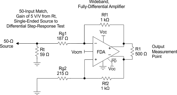
The output considerations remain the same as for the AC-coupled design. Again, the input can be DC-coupled while the output is AC-coupled. A DC-coupled input with an AC-coupled output might have some advantages to move the input VICM down if the source is ground referenced. When the source is DC-coupled into the THS4531A family (see Figure 97), both sides of the input circuit must be DC-coupled to retain differential balance. Normally, the nonsignal input side has an RG element biased to whatever the source midrange is expected to be. Providing this midscale reference gives a balanced differential swing around VOCM at the outputs.
Often, RG2 is simply grounded for DC-coupled, bipolar-input applications. This configuration gives a balanced differential output if the source is swinging around ground. If the source swings from ground to some positive voltage, grounding RG2 gives a unipolar output differential swing from both outputs at VOCM (when the input is at ground) to one polarity of swing. Biasing RG2 to an expected midpoint for the input signal creates a differential output swing around VOCM.
One significant consideration for a DC-coupled input is that VOCM sets up a common-mode bias current from the output back through RF and RG to the source on both sides of the feedback. Without input balancing networks, the source must sink or source this DC current. After the input signal range and biasing on the other RG element is set, check that the voltage divider from VOCM to VIN through RF and RG (and possibly RS) establishes an input VICM at the device input pins that is in range.
If the average source is at ground, the negative rail input stage for the THS4531A family is in range for applications using a single positive supply and a positive output VOCM setting because this DC current lifts the average FDA input summing junctions up off of ground to a positive voltage (the average of the V+ and V– input pin voltages on the FDA).
 Figure 97. DC-Coupled, Single-Ended-to-Differential, Set for a Gain of 5 V/V