SLOS823D December 2012 – March 2020 THS4531A
PRODUCTION DATA.
- 1 Features
- 2 Applications
- 3 Description
- 4 Revision History
- 5 Related Products
- 6 Pin Configuration and Functions
- 7 Specifications
- 8 Detailed Description
-
9 Application and Implementation
- 9.1
Application Information
- 9.1.1 Frequency Response, and Output Impedance
- 9.1.2 Distortion
- 9.1.3 Slew Rate, Transient Response, Settling Time, Overdrive, Output Voltage, and Turnon and Turnoff Time
- 9.1.4 Common-Mode and Power Supply Rejection
- 9.1.5 VOCM Input
- 9.1.6 Balance Error
- 9.1.7 Single-Supply Operation
- 9.1.8 Low-Power Applications and the Effects of Resistor Values on Bandwidth
- 9.1.9 Driving Capacitive Loads
- 9.1.10 Audio Performance
- 9.1.11 Audio On and Off Pop Performance
- 9.2
Typical Applications
- 9.2.1 SAR ADC Performance: THS4531A and ADS8321 Combined Performance
- 9.2.2 Audio ADC Driver Performance: THS4531A and PCM4204 Combined Performance
- 9.2.3 SAR ADC Performance: THS4531A and ADS7945 Combined Performance
- 9.2.4 Differential-Input to Differential-Output Amplifier
- 9.2.5 Single-Ended to Differential FDA Configuration
- 9.2.6 Single-Ended Input to Differential Output Amplifier
- 9.2.7 Differential Input to Single-Ended Output Amplifier
- 9.1
Application Information
- 10Power Supply Recommendations
- 11Layout
- 12Device and Documentation Support
- 13Mechanical, Packaging, and Orderable Information
Package Options
Mechanical Data (Package|Pins)
Thermal pad, mechanical data (Package|Pins)
Orderable Information
9.1.8 Low-Power Applications and the Effects of Resistor Values on Bandwidth
The THS4531A is designed for the nominal value of RF to be 2 kΩ. This gives excellent distortion performance, maximum bandwidth, best flatness, and best pulse response. It also loads the amplifier. For example; in gain of 1 with RF = RG = 2 kΩ, RG to ground, and VOUT+ = 4 V, 1 mA of current will flow through the feedback path to ground. In low power applications, reducing this current is desirable by increasing the gain setting resistors values. Using larger value gain resistors has three primary side effects (other than lower power) because of the interaction with the device and PCB parasitic capacitance:
- Lowers the bandwidth.
- Lowers the phase margin.
- This causes peaking in the frequency response.
- This also causes overshoot and ringing in the pulse response.
- Increases the output noise.
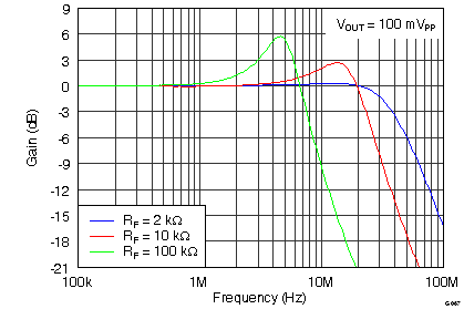
Figure 76 shows the small signal frequency response for gain of 1 with RF and RG equal to 2 kΩ, 10 kΩ, and 100 kΩ. The test was done with RL = 2 kΩ. Because of loading effects of RL, lower values may reduce the peaking, but higher values will not have a significant effect.
As expected, larger value gain resistors cause lower bandwidth and peaking in the response (peaking in frequency response is synonymous with overshoot and ringing in pulse response). These effects are caused by the feedback pole created by the summing-junction capacitance and these larger Rf values.
 Figure 76. THS4531A Frequency Response with Various Gain Setting Resistor Values