SLOS823D December 2012 – March 2020 THS4531A
PRODUCTION DATA.
- 1 Features
- 2 Applications
- 3 Description
- 4 Revision History
- 5 Related Products
- 6 Pin Configuration and Functions
- 7 Specifications
- 8 Detailed Description
-
9 Application and Implementation
- 9.1
Application Information
- 9.1.1 Frequency Response, and Output Impedance
- 9.1.2 Distortion
- 9.1.3 Slew Rate, Transient Response, Settling Time, Overdrive, Output Voltage, and Turnon and Turnoff Time
- 9.1.4 Common-Mode and Power Supply Rejection
- 9.1.5 VOCM Input
- 9.1.6 Balance Error
- 9.1.7 Single-Supply Operation
- 9.1.8 Low-Power Applications and the Effects of Resistor Values on Bandwidth
- 9.1.9 Driving Capacitive Loads
- 9.1.10 Audio Performance
- 9.1.11 Audio On and Off Pop Performance
- 9.2
Typical Applications
- 9.2.1 SAR ADC Performance: THS4531A and ADS8321 Combined Performance
- 9.2.2 Audio ADC Driver Performance: THS4531A and PCM4204 Combined Performance
- 9.2.3 SAR ADC Performance: THS4531A and ADS7945 Combined Performance
- 9.2.4 Differential-Input to Differential-Output Amplifier
- 9.2.5 Single-Ended to Differential FDA Configuration
- 9.2.6 Single-Ended Input to Differential Output Amplifier
- 9.2.7 Differential Input to Single-Ended Output Amplifier
- 9.1
Application Information
- 10Power Supply Recommendations
- 11Layout
- 12Device and Documentation Support
- 13Mechanical, Packaging, and Orderable Information
Package Options
Mechanical Data (Package|Pins)
Thermal pad, mechanical data (Package|Pins)
Orderable Information
9.2.6.3 Resistor Design Equations for the Single-Ended to Differential Configuration of the FDA
The design equations for setting the resistors around an FDA to convert from a single-ended input signal to differential output can be approached from several directions. Here, several critical assumptions are made to simplify the results:
- The feedback resistors are selected first and set equal on the two sides.
- The DC and AC impedances from the summing junctions back to the signal source and ground (or a bias voltage on the nonsignal input side) are set equal to retain feedback divider balance on each side of the FDA.
Both of these assumptions are typical for delivering the best dynamic range through the FDA signal path.
After the feedback resistor values are chosen, the aim is to solve for the RT (a termination resistor to ground on the signal input side), RG1 (the input gain resistor for the signal path), and RG2 (the matching gain resistor on the nonsignal input side); see Figure 96 and Figure 97. The same resistor solutions can be applied to either AC- or DC-coupled paths. Adding blocking capacitors in the input-signal chain is a simple option. Adding these blocking capacitors after the RT element (as shown in Figure 96) has the advantage of removing any DC currents in the feedback path from the output VOCM to ground.
Earlier approaches to the solutions for RT and RG1 (when the input must be matched to a source impedance, RS) follow an iterative approach. This complexity arises from the active input impedance at the RG1 input. When the FDA is used to convert a single-ended signal to differential, the common-mode input voltage at the FDA inputs must move with the input signal to generate the inverted output signal as a current in the RG2 element. A more recent solution is shown as Equation 8, where a quadratic in RT can be solved for an exact value. This quadratic emerges from the simultaneous solution for a matched input impedance and target gain. The only inputs required are:
- The selected RF value.
- The target voltage gain (Av) from the input of RT to the differential output voltage.
- The desired input impedance at the junction of RT and RG1 to match RS.
Solving this quadratic for RT starts the solution sequence, as shown in Equation 8:

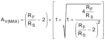
Being a quadratic, there are limits to the range of solutions. Specifically, after RF and RS are chosen, there is physically a maximum gain beyond which Equation 8 starts to solve for negative RT values (if input matching is a requirement). With RF selected, use Equation 9 to verify that the maximum gain is greater than the desired gain.

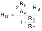
If the achievable AV(MAX) is less than desired, increase the RF value. After RT is derived from Equation 8, the RG1 element is given by Equation 10:

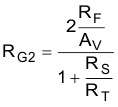
Then, the simplest approach is to use a single RG2 = RT || RS + RG1 on the nonsignal input side. Often, this approach is shown as the separate RG1 and RS elements. Using these separate elements provides a better divider match on the two feedback paths, but a single RG2 is often acceptable. A direct solution for RG2 is given as Equation 11:

This design proceeds from a target input impedance matched to RS, signal gain Av from the matched input to the differential output voltage, and a selected RF value. The nominal RF value chosen for the THS4531A family characterization is 2 kΩ. As discussed previously, going lower improves noise and phase margin, but reduces the total output load impedance possibly degrading harmonic distortion. Going higher increases the output noise, and might reduce the loop-phase margin because of the feedback pole to the input capacitance, but reduces the total loading on the outputs.
Using Equation 9 to Equation 11 to sweep the target gain from 1 to AV(MAX) < 10 V/V gives Table 9, which shows exact values for RT, RG1, and RG2, where a 50-Ω source must be matched while setting the two feedback resistors to 2 kΩ. One possible solution for 1% standard values is shown, and the resulting actual input impedance and gain with % errors to the targets are also shown in Table 9.
Table 9. Rf = 2 kΩ, Matched Input to 50 Ω, Gain of 1 to 10-V/V Single-Ended to Differential(1)
| Av | Rt, EXACT (Ω) | Rt 1% | Rg1, EXACT (Ω) | Rg1 1% | Rg2, EXACT (Ω) | Rg2 1% | ACTUAL ZIN | %ERR TO Rs | ACTUAL GAIN | %ERR TO Av |
|---|---|---|---|---|---|---|---|---|---|---|
| 1 | 51 | 51.1 | 1996.5 | 2000 | 2021.8 | 2000 | 50.1 | 0.3 | 0.998 | –0.2 |
| 2 | 51.7 | 52.3 | 996.9 | 1000 | 1022.5 | 1020 | 50.5 | 1.0 | 1.994 | –0.3 |
| 3 | 52.5 | 52.3 | 656.1 | 649 | 681.7 | 681 | 49.7 | –0.5 | 3.032 | 1.1 |
| 4 | 53.2 | 53.6 | 491.5 | 487 | 517.4 | 523 | 50.2 | 0.4 | 4.035 | 0.9 |
| 5 | 54 | 53.6 | 388 | 392 | 413.9 | 412 | 49.6 | –0.9 | 4.953 | –0.9 |
| 6 | 54.7 | 54.9 | 322.7 | 324 | 348.9 | 348 | 49.9 | –0.2 | 5.978 | –0.4 |
| 7 | 55.5 | 54.9 | 272.9 | 274 | 299.1 | 301 | 49.1 | –1.7 | 6.974 | –0.4 |
| 8 | 56.3 | 56.2 | 238.1 | 237 | 264.6 | 267 | 49.3 | –1.3 | 8.034 | 0.4 |
| 9 | 57.1 | 57.6 | 211.2 | 210 | 237.9 | 237 | 49.7 | –0.6 | 9.044 | 0.5 |
| 10 | 57.9 | 57.6 | 187.4 | 187 | 214.1 | 215 | 48.9 | –2.3 | 10.017 | 0.2 |
These equations and design flow apply to any FDA. Using the feedback resistor value as a starting point is particularly useful for current-feedback-based FDAs such as the LMH6554, where the value of these feedback resistors determines the frequency response flatness. Similar tables can be built using the equations provided here for other source impedances, RF values, and gain ranges.
The TINA model correctly shows this actively-set input impedance in the single-ended to differential configuration, and is a good tool to validate the gains, input impedances, response shapes, and noise issues.