SBOS778D April 2016 – April 2021 THS4551
PRODUCTION DATA
- 1 Features
- 2 Applications
- 3 Description
- 4 Revision History
- 5 Companion Devices
- 6 Pin Configuration and Functions
-
7 Specifications
- 7.1 Absolute Maximum Ratings
- 7.2 ESD Ratings
- 7.3 Recommended Operating Conditions
- 7.4 Thermal Information
- 7.5 Electrical Characteristics: (VS+) – (VS–) = 5 V
- 7.6 Electrical Characteristics: (VS+) – (VS–) = 3 V
- 7.7 Typical Characteristics: (VS+) – (VS–) = 5 V
- 7.8 Typical Characteristics: (VS+) – (VS–) = 3 V
- 7.9 Typical Characteristics: 3-V to 5-V Supply Range
-
8 Parameter Measurement Information
- 8.1 Example Characterization Circuits
- 8.2 Output Interface Circuit for DC-Coupled Differential Testing
- 8.3 Output Common-Mode Measurements
- 8.4 Differential Amplifier Noise Measurements
- 8.5 Balanced Split-Supply Versus Single-Supply Characterization
- 8.6 Simulated Characterization Curves
- 8.7 Terminology and Application Assumptions
- 9 Detailed Description
- 10Application and Implementation
- 11Power Supply Recommendations
- 12Layout
- 13Device and Documentation Support
- 14Mechanical, Packaging, and Orderable Information
Package Options
Mechanical Data (Package|Pins)
Thermal pad, mechanical data (Package|Pins)
Orderable Information
10.1.6 Designing Attenuators
Operating the THS4551 at a low-noise gain (or with higher feedback resistors) can cause a lower phase margin to exist, thus giving the response peaking illustrated in Figure 7-1 for the gain of a 0.1 (a 1/10 attenuator) condition. Although operating the THS4551 as an attenuator is often useful, taking a large input range to a controlled output common-mode voltage with a purely differential signal around the VOCM voltage, the response peaking illustrated in Figure 7-1 is usually undesirable. Several approaches can be used to reduce or eliminate this peaking, usually at the cost of higher output noise. DC attenuation at the input usually increases the output noise broadband, whereas using an ac noise gain shaping technique that peaks the noise gain only at higher frequencies is more desirable. This peaking output noise can then be filtered off with the typical passive RC filters often used after this stage. Figure 10-4 shows a simplified schematic for the gain of 0.1-V/V test from Figure 7-1.
 Figure 10-4 Divide-by-10 Attenuator Application for the THS4551
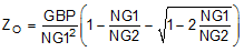
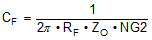
A 5-dB peaked response (see Figure 10-6) results from the configuration of Figure 10-4, which results from a nominal 32° phase margin. This peaking can be eliminated by placing two feedback capacitors across the RF elements and a differential input capacitor. Adding these capacitors provides a transition from a resistively set noise gain (NG1 = 1.1 in Figure 10-4) to a capacitive divider at high frequency, and flattening out to a higher noise gain (NG2). The key for this approach is to target a ZO where the noise gain begins to peak up. Using only the following terms, and targeting a closed-loop flat (Butterworth) response, gives this solution sequence (from Equation 11 to Equation 13) for ZO and then the capacitor values. See the OPA847 data sheet (page 12) for a discussion of this inverting noise gain shaping technique.
- Gain bandwidth product in Hz (135 MHz for the THS4551)
- Low-frequency noise gain, NG1 (equal to 1.1 in the attenuator gain of a 0.1-V/V design)
- The target high-frequency noise gain is selected to be higher than NG1 (NG2 = 5 V/V) in this example
- Feedback resistor value, RF (is assumed balanced for this differential design = 1 kΩ)
From these elements, for any voltage feedback op amp or FDA, solve for ZO as shown in Equation 11:
From this target zero frequency in the noise gain, the feedback capacitors can be solved as Equation 12:
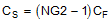
The next step is to resolve the input capacitance on the summing junction. Equation 13 is for a single-ended op amp where the capacitor goes to ground. To use the capacitance (CS) resulting from Equation 13 for a voltage-feedback FDA, cut the target value in half and place the resulting CS across the two inputs (reducing the external value by the specified internal differential capacitance).
Using the computed capacitor values allows for an estimate of the resulting flat response bandwidth f–3dB frequency, as shown in Equation 14:
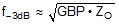
Running through these steps for the THS4551 in the attenuator circuit of Figure 10-4 provides the proposed compensation of Figure 10-5, where Equation 14 estimates a bandwidth of 22 MHz (the ZO target is 3.5 MHz). The solutions for CF gives 9 pF, where this value is reduced to 8.4 pF to account for the internal 0.6-pF feedback. The single-ended solution for CS gives 36 pF, which is reduced to 18 pF to be differential, and is then further reduced to 16.8 pF to account for the internal 1.2-pF differential input capacitance of the THS4551.
 Figure 10-5 Compensated Attenuator Circuit Using the THS4551
The 16.8 pF across the inputs is really a total of 36 pF for a single-ended design from Equation 13 reduced by half and then the 1.2-pF internal capacitance is removed.
These two designs (with and without the compensation capacitors) were both bench tested and simulated using the THS4551 TINA-TI™ model, which resulted in Figure 10-6. The TINA-TI™ simulation files used for Figure 10-6 are available both without the compensation capacitors and with the capacitors in place.
 Figure 10-6 Attenuator Response Shapes With and Without External Capacitors
This approach does a good job of flattening the response for what starts out as a low phase margin attenuator application. The simulation model does a very good job of predicting the peaking and showing the same improvement with the external capacitors (both give a flat, approximately 24-MHz, closed-loop bandwidth for the gain of 0.1-V/V design). The output noise starts to peak up (because of the noise gain shaping of the capacitors) above 3.5 MHz in this example. These stages normally drive the RC filter at the input of a SAR ADC that filters off the noise peaking above 3.5 MHz.