SBOS778D April 2016 – April 2021 THS4551
PRODUCTION DATA
- 1 Features
- 2 Applications
- 3 Description
- 4 Revision History
- 5 Companion Devices
- 6 Pin Configuration and Functions
-
7 Specifications
- 7.1 Absolute Maximum Ratings
- 7.2 ESD Ratings
- 7.3 Recommended Operating Conditions
- 7.4 Thermal Information
- 7.5 Electrical Characteristics: (VS+) – (VS–) = 5 V
- 7.6 Electrical Characteristics: (VS+) – (VS–) = 3 V
- 7.7 Typical Characteristics: (VS+) – (VS–) = 5 V
- 7.8 Typical Characteristics: (VS+) – (VS–) = 3 V
- 7.9 Typical Characteristics: 3-V to 5-V Supply Range
-
8 Parameter Measurement Information
- 8.1 Example Characterization Circuits
- 8.2 Output Interface Circuit for DC-Coupled Differential Testing
- 8.3 Output Common-Mode Measurements
- 8.4 Differential Amplifier Noise Measurements
- 8.5 Balanced Split-Supply Versus Single-Supply Characterization
- 8.6 Simulated Characterization Curves
- 8.7 Terminology and Application Assumptions
- 9 Detailed Description
- 10Application and Implementation
- 11Power Supply Recommendations
- 12Layout
- 13Device and Documentation Support
- 14Mechanical, Packaging, and Orderable Information
Package Options
Mechanical Data (Package|Pins)
Thermal pad, mechanical data (Package|Pins)
Orderable Information
3 Description
The THS4551 fully differential amplifier offers an easy interface from single-ended sources to the differential output required by high-precision analog-to-digital converters (ADCs). Designed for exceptional dc accuracy, low noise, and robust capacitive load driving, this device is well suited for data acquisition systems where high precision is required along with the best signal-to-noise ratio (SNR) and spurious-free dynamic range (SFDR) through the amplifier and ADC combination.
The THS4551 features the negative rail input required when interfacing a dc-coupled, ground-centered, source signal to a single-supply differential input ADC. Very low dc error and drift terms support the emerging 16- to 20-bit successive-approximation register (SAR) input requirements. A wide-range output common-mode control supports the ADC running from 1.8-V to 5-V supplies with ADC common-mode input requirements from 0.7 V to greater than 3.0 V.
The THS4551 device is characterized for operation over the wide temperature range of –40°C to +125°C, and is available in 8-pin VSSOP, 16-pin VQFN, and 10-pin WQFN packages.
| PART NUMBER | PACKAGE | BODY SIZE (NOM) |
|---|---|---|
| THS4551 | VSSOP (8) | 3.00 mm × 3.00 mm |
| WQFN (10) | 2.00 mm × 2.00 mm | |
| VQFN (16) | 3.00 mm × 3.00 mm |
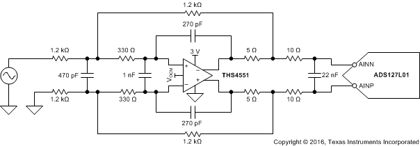
 Simplified Schematic: Gain of 1 V/V, Single-Ended Input to Differential Output,
500-kHz, Multiple Feedback Filter Interface to the ADS127L01