SBOS778D April 2016 – April 2021 THS4551
PRODUCTION DATA
- 1 Features
- 2 Applications
- 3 Description
- 4 Revision History
- 5 Companion Devices
- 6 Pin Configuration and Functions
-
7 Specifications
- 7.1 Absolute Maximum Ratings
- 7.2 ESD Ratings
- 7.3 Recommended Operating Conditions
- 7.4 Thermal Information
- 7.5 Electrical Characteristics: (VS+) – (VS–) = 5 V
- 7.6 Electrical Characteristics: (VS+) – (VS–) = 3 V
- 7.7 Typical Characteristics: (VS+) – (VS–) = 5 V
- 7.8 Typical Characteristics: (VS+) – (VS–) = 3 V
- 7.9 Typical Characteristics: 3-V to 5-V Supply Range
-
8 Parameter Measurement Information
- 8.1 Example Characterization Circuits
- 8.2 Output Interface Circuit for DC-Coupled Differential Testing
- 8.3 Output Common-Mode Measurements
- 8.4 Differential Amplifier Noise Measurements
- 8.5 Balanced Split-Supply Versus Single-Supply Characterization
- 8.6 Simulated Characterization Curves
- 8.7 Terminology and Application Assumptions
- 9 Detailed Description
- 10Application and Implementation
- 11Power Supply Recommendations
- 12Layout
- 13Device and Documentation Support
- 14Mechanical, Packaging, and Orderable Information
Package Options
Mechanical Data (Package|Pins)
Thermal pad, mechanical data (Package|Pins)
Orderable Information
9.3.4 Output DC Error and Drift Calculations and the Effect of Resistor Imbalances
The THS4551 offers a trimmed input offset voltage and extremely low offset drift over the full –40°C to +125°C operating range. This offset voltage combines with several other error contribution terms to produce an initial 25°C output offset error band and then a drift over temperature. For each error term, a gain must be assigned to that term. For this analysis, only dc-coupled signal paths are considered. One new source of output error (versus the typical op amp analysis) arises from the effect mismatched resistor values and ratios can have on the two sides of the FDA. Any common-mode error or drift creates a differential output error through the slight mismatches arising from the external feedback and gain setting resistor tolerances or standard value constraints.
The error terms (25°C and drift), along with the gain to the output differential voltage, include input offset voltage and input offset current. Input offset voltage has a gain equal to the noise gain or 1 + RF / RG, where RG is the total dc impedance from the input pins back to the source or a dc reference (typically ground). Input offset current has a gain to the differential output through the average feedback resistor value.
The remaining terms arise from an assumed range on both the absolute feedback resistor mismatch and the mismatch in the divider ratio on each side of the FDA. The first of these resistor mismatch terms is the input bias current that creates a differential output offset via RF mismatch. For simplicity, the upper RF and RG values are termed RF1 and RG1 with a ratio of RF1 / RG1 ≡ G1. The lower elements are defined as RF2 and RG2 with a ratio of RF2 / RG2 ≡ G2. To compute worst-case contributions, a maximum variation in the design resistor tolerance is used in the absolute and ratio mismatches.
For instance, ±1% tolerance resistors are assumed, giving a worst-case G1 that is 2% higher than nominal and a G2 that is 2% lower than nominal with a worst-case RF value mismatch of 2% as well. Using a 0.1% precision resistor reduces the gain for the input bias current, but because these precision resistors are usually only available in 1% value steps, a gain mismatch term may still need to be considered. For matched impedance designs with RT and RG1 on a single-ended to differential stage, the standard value constraint imposes a fixed mismatch in the initial feedback ratios with the tolerance of the resistors around the ratio if the non-signal input side uses a single resistor for RG2.
Define the selected external resistor tolerance as ±T (so for 1% tolerance resistors, T = 0.01). Input bias current times the feedback resistor mismatch gain is ±2 × T × RFnom.
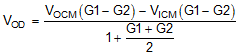
Anything that generates an output common-mode level or shift over temperature also generates an output differential error term if the two feedback ratios, G1 and G2, are not equal. An error trying to produce a shift in the output common-mode voltage is overridden by the common-mode control loop where the error becomes a balanced differential error around the output VOCM.
The terms that create a differential error from a common-mode term and feedback ratio mismatch include the desired VOCM voltage, any source common-mode voltage, any drift on the reference bias to the VOCM control pin, any internal offset and drift in the VOCM control path, and the input average bias current and drift.
Considering just the output common-mode control and the source common-mode voltage, the conversion to output differential offsets is through Equation 8.
Neglecting any G1 and G2 mismatch because of standard values constraint, the conversion gain for these two terms can be recast in terms of the nominal RF / RG ≡ G and the tolerance T, as shown in Equation 9. When G increases, this conversion gain approaches 4T.
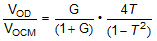
This conversion gain to differential output error is applied to two error terms: VOCM and the input bias current and drift. (The source common-mode voltage is assumed to be 0 V. If not, apply this gain to the source common-mode voltage and any resulting shift in application.)
The output error is applied to VOCM, assuming that the input control pin is driven and not floating. The input bias current and drift are multiplied by the average RF value then by the conversion gain to differential output error to create an added output differential error.
As an example of using these terms to estimate the worst-case output 25°C error band and then the worst-case drift (by adding all error terms together independently), use the gain of 1-V/V configuration with RF = 1 kΩ and assume a ±1% tolerance on the resistors with the standard values used in Figure 9-9.
 Figure 9-9 DC-Coupled Gain of 1 with RF = 1 kΩ and Single-to-Differential Matched Input 50-Ω Impedance
The standard value constraint on the non-signal input side actually produces more gain mismatch than the resistor tolerances. For Figure 9-9, G2 = 1000 / 1020 = 0.9804 and G1 = 1000 / 1025.6 = 0.9751 nominally, then with a ±2% tolerance around the initial gain mismatch resulting from the standard values available if 1% resistors are used.
Using the maximum 25°C error terms and nominal resistor values with an exact 2.5-V input to the VOCM control pin gives Table 9-2, gains to the output differential error (VOD), and then the summed output error band at 25°C. The output error is clearly dominated by the VOCM voltage and the effect of the nominal feedback dividers being slightly mismatched. This analysis does not include resistor tolerances but the approach is the same with the wider error bands on the gain terms. Using 1% tolerance on the resistors setting the gain matching dominates the output error band through the VOCM input voltage. For the lowest output error, this analysis shows that an exact match on the feedback dividers with precision resistors is preferred. However, doing so would require duplicating the exact network on the non-signal input side and the signal input side. Where input impedance matching is not required, the two RG resistors are simply single equal resistors and the gain mismatch is just from the tolerance of the resistors.
| ERROR TERM | 25°C MAX VALUE | GAIN TO VOD | OUTPUT ERROR (mV) | GAIN COMMENT |
|---|---|---|---|---|
| Input VIO | ±0.175 mV | 1.9777 | ±0.346 | Average noise gain |
| Input IOS | ±50 nA | 1000 | ±0.05 | Feedback resistor |
| Input IBCM | 1.5 µA | 20 Ω | ±0.03 | Feedback resistor mismatch |
| Input IBCM | 1.5 µA | 1 kΩ × 0.00268 | ±0.004 | Converted to differential by gain mismatch |
| VOCM input | 2.5 V | 0.00268 | ±6.7 | VOCM to differential by gain mismatch |
| Total | ±7.13 |
The 0.00268 conversion gain for the gain ratio mismatch is the worst-case ratio starting from the initially lower G1 value resulting from the standard value constraint and using a ±1% tolerance on the RF and RG elements of the ratio. Adding in the resistor tolerances to the gain mismatch term greatly increases the contribution of those terms.
Normally, the expected drift in the output VOD is of more interest than an initial error band. Table 9-3 shows these terms for the RGT package and the summed results by adding all terms independently to obtain a worst-case drift.
| ERROR TERM | MAX VALUE | GAIN TO VOD | OUTPUT ERROR (µV/°C) | GAIN COMMENT |
|---|---|---|---|---|
| Input VIO | ±1.8 µV/°C | 1.9777 | ±3.56 | Average noise gain |
| Input IOS | ±120 pA/°C | 1000 | ±0.12 | Feedback resistor |
| Input IBCM | 5.0 nA/°C | 20 Ω | ±0.10 | Feedback resistor mismatch |
| Input IBCM | 5.0 nA/°C | 1 kΩ × 0.00268 | ±0.013 | Converted to differential by gain mismatch |
| VOCM input | ±10 µV/°C | 0.00268 | ±0.027 | VOCM to differential by gain mismatch |
| Total | ±3.82 |
In Table 9-3, the input offset voltage drift dominates the output drift. For the last term, the drift for the VOCM path is just for the internal offset drift of the common-mode path with a driven input. Any added external drift on the source of the VOCM input must also be considered. This type of calculation can be repeated for the exact application circuit considering each of these terms in the context of a specific design.
The absolute accuracy and drift for the THS4551 are exceptionally good. Mismatched resistor feedback ratios combined with a high drift in the VOCM control input can actually dominate the output VOD drift. Where the output differential precision is more important than the input matching accuracy, consider matching the networks on the two sides of the input to obtain improved nominal G1 to G2 match. The gains for the input bias current error terms are relatively low when using the 1-kΩ feedback values. Higher RF values provide the input-current-related drift terms more gain.