SBOS874D August 2017 – February 2021 THS4561
PRODUCTION DATA
- 1 Features
- 2 Applications
- 3 Description
- 4 Revision History
- 5 Device Comparison Table
- 6 Pin Configuration and Functions
-
7 Specifications
- 7.1 Absolute Maximum Ratings
- 7.2 ESD Ratings
- 7.3 Recommended Operating Conditions
- 7.4 Thermal Information
- 7.5 Electrical Characteristics: VS+ – VS– = 5 V to 12 V
- 7.6 Typical Characteristics: (VS+) – (VS–) = 12 V
- 7.7 Typical Characteristics: (VS+) – (VS–) = 5 V
- 7.8 Typical Characteristics: (VS+) – (VS–) = 3 V
- 7.9 Typical Characteristics: (VS+) – (VS–) = 3-V to 12-V Supply Range
-
8 Parameter Measurement Information
- 8.1 Example Characterization Circuits
- 8.2 Output Interface Circuit for DC-Coupled Differential Testing
- 8.3 Output Common-Mode Measurements
- 8.4 Differential Amplifier Noise Measurements
- 8.5 Balanced Split-Supply Versus Single-Supply Characterization
- 8.6 Simulated Characterization Curves
- 8.7 Terminology and Application Assumptions
- 9 Detailed Description
- 10Application and Implementation
- 11Power Supply Recommendations
- 12Layout
- 13Device and Documentation Support
- 14Mechanical, Packaging, and Orderable Information
Package Options
Mechanical Data (Package|Pins)
Thermal pad, mechanical data (Package|Pins)
Orderable Information
8.3 Output Common-Mode Measurements
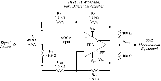
The circuit of Figure 8-5 is a typical setup for common-mode measurements.
 Figure 8-5 Output Common-Mode Measurements
In Figure 8-5, the differential path is terminated back to ground with the two 1.5-kΩ input resistors and the VOCM control input is driven from a 50-Ω matched source for the frequency response and step response curves of Figure 7-47, Figure 7-49, and Figure 7-50. The outputs are summed to a center point (to obtain the average, or common-mode output, VOCM) through two 100-Ω resistors. These 100-Ω resistors form an equivalent 50-Ω source to the common-mode output for measurements. Figure 7-48 illustrates the common-mode output noise measurements with a ground on the VOCM input pin or with the VOCM input pin floating. The higher noise in Figure 7-48 for a floated input can be reduced by including a capacitor to ground at the VOCM control input pin.