SBOSA51 December 2020 THS4567
PRODUCTION DATA
- 1 Features
- 2 Applications
- 3 Description
- 4 Revision History
- 5 Pin Configuration and Functions
- 6 Specifications
- 7 Detailed Description
- 8 Application and Implementation
- 9 Power Supply Recommendations
- 10Layout
- 11Device and Documentation Support
- 12Mechanical, Packaging, and Orderable Information
Package Options
Mechanical Data (Package|Pins)
- RUN|10
Thermal pad, mechanical data (Package|Pins)
- RUN|10
Orderable Information
8.2.2 Detailed Design Procedure (THS4567 in TIA Mode)
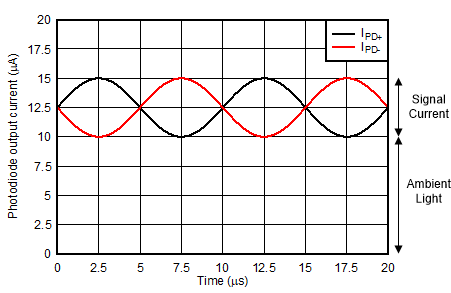
The output current from each photodiode is shown in Figure 8-4. A detailed procedure on how to set the various bias voltages and select the optimal value of transimpedance gain follows.
- Set VS+ = 5.25 V and VS– = –0.25 V to allow the THS4567 to swing 10 VPP (differential) without introducing distortion due to limited headroom.
- Set ICM_EN = logic high to enable the THS4567 TIA mode of operation.
- Set VOCM to 2.5 V to match the ADC input common-mode range.
- With the photodiodes (PDs) configured with a cathode bias as shown in Figure 8-2 both PDs will source current when light is incident on them. To maximize the reverse bias across the PD, VBIAS is typically set to the amplifiers positive supply voltage or the highest available positive supply voltage.
- The maximum output current from
the PD is the sum of the ambient light current and the maximum signal current.
Equation 2. ITOTAL = IAMBIENT + ISIGNAL = 10 µA + 5 µA = 15 µA
- In
the TIA mode, VICM is set to its minimum input common-mode compliance limit
(1.25 V) to maximize the reverse bias across the PDs thereby reducing the PD
capacitance. Equation 3. Reverse bias across the photodiodes = (5.25 V - 1.25 V) = 4 V
- In the TIA mode, the ICM loop
cancels the common-mode input current due to ambient light (10 µA) at the
amplifier's input pin and only the differential signal current flows through the
feedback resistors RF and RF'. The maximum TIA gain is
therefore the ratio of the maximum differential output swing and the maximum
differential signal current as shown in Equation 4. Equation 4. Maximum TIA gain = (10 VPP/ 10 µA) = 1 MΩ
- Once the feedback resistor value is set, select the value of feedback capacitance as described in Transimpedance Considerations for High-Speed Amplifiers.
 Figure 8-4 Photodiode Differential Output Current