SBOS974D August 2019 – April 2021 THS6222
PRODUCTION DATA
- 1 Features
- 2 Applications
- 3 Description
- 4 Revision History
- 5 Pin Configuration and Functions
- 6 Specifications
- 7 Detailed Description
- 8 Application and Implementation
- 9 Power Supply Recommendations
- 10Layout
- 11Device and Documentation Support
- 12Mechanical, Packaging, and Orderable Information
Package Options
Mechanical Data (Package|Pins)
Thermal pad, mechanical data (Package|Pins)
- RGT|16
Orderable Information
3 Description
The THS6222 is a differential line-driver amplifier with a current-feedback architecture manufactured using Texas Instruments' proprietary, high-speed, silicon-germanium (SiGe) process. The device is targeted for use in broadband, high-speed, power line communications (HPLC) line driver applications that require high linearity when driving heavy line loads.
The unique architecture of the THS6222 uses minimal quiescent current while achieving very high linearity. The amplifier has an adjustable current pin (IADJ) that sets the nominal current consumption along with the multiple bias modes that allow for enhanced power savings where the full performance of the amplifier is not required. Shutdown bias mode provides further power savings during receive mode in time division multiplexed (TDM) systems while maintaining high output impedance. The integrated midsupply common-mode buffer eliminates external components, reducing system cost and board space.
The wide output swing of
57 VPP (100 Ω load) with
32-V power
supplies, coupled with over 650 mA current drive (25 Ω load), allows for wide
dynamic range that keeps distortion minimal.
The THS6222 is available in a 24-pin VQFN package with exposed thermal pad and is specified for operation from –40°C to +85°C ambient temperature.
| PART NUMBER | PACKAGE(1) | BODY SIZE (NOM) |
|---|---|---|
| THS6222 | VQFN (24) | 5.00 mm × 4.00 mm |
| Wafer Sale (19) | 1261.00 µm × 1641.00 µm | |
| VQFN (16) | 3.0 mm × 3.0 mm |
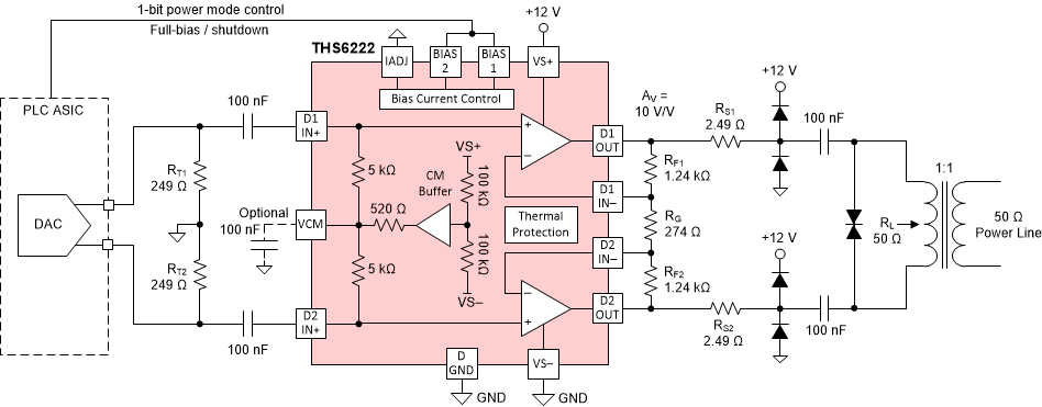
 Typical Line-Driver Circuit
Using the THS6222