SLLSFQ4A September 2022 – March 2023 THVD1424
PRODUCTION DATA
- 1 Features
- 2 Applications
- 3 Description
- 4 Revision History
- 5 Pin Configuration and Functions
-
6 Specifications
- 6.1 Absolute Maximum Ratings
- 6.2 ESD Ratings
- 6.3 ESD Ratings [IEC]
- 6.4 Recommended Operating Conditions
- 6.5 Thermal Information
- 6.6 Power Dissipation
- 6.7 Electrical Characteristics
- 6.8 Switching Characteristics_500 kbps
- 6.9 Switching Characteristics_20 Mbps
- 6.10 Switching Characteristics_Termination resistor
- 6.11 Switching Characteristics_Duplex switching
- 6.12 Typical Characteristics
- 7 Parameter Measurement Information
- 8 Detailed Description
- 9 Application Information Disclaimer
- 10Device and Documentation Support
- 11Mechanical, Packaging, and Orderable Information
Package Options
Mechanical Data (Package|Pins)
- RGT|16
Thermal pad, mechanical data (Package|Pins)
- RGT|16
Orderable Information
9.2.1.5 Transient Protection
The bus pins of the THVD1424 transceiver family include on-chip ESD protection against ±16-kV HBM and ±8-kV IEC 61000-4-2 contact discharge. The International Electrotechnical Commission (IEC) ESD test is far more severe than the HBM ESD test. The 50% higher charge capacitance, C(S), and 78% lower discharge resistance, R(D), of the IEC model produce significantly higher discharge currents than the HBM model.
 Figure 9-3 HBM and IEC ESD Models and Currents in Comparison (HBM Values in Parenthesis)
The on-chip implementation of IEC ESD protection significantly increases the robustness of equipment. Common discharge events occur because of human contact with connectors and cables. Designers may choose to implement protection against longer duration transients, typically referred to as surge transients.
EFTs are generally caused by relay-contact bounce or the interruption of inductive loads. Surge transients often result from lightning strikes (direct strike or an indirect strike which induce voltages and currents), or the switching of power systems, including load changes and short circuit switching. These transients are often encountered in industrial environments, such as factory automation and power-grid systems.
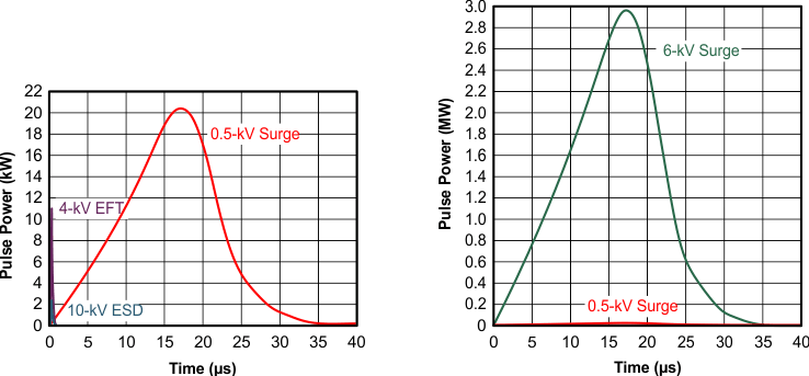
Figure 9-4 compares the pulse-power of the EFT and surge transients with the power caused by an IEC ESD transient. The left hand diagram shows the relative pulse-power for a 0.5-kV surge transient and 4-kV EFT transient, both of which dwarf the 10-kV ESD transient visible in the lower-left corner. 500-V surge transients are representative of events that may occur in factory environments in industrial and process automation.
The right side diagram shows the pulse-power of a 6-kV surge transient, relative to the same 0.5-kV surge transient. 6-kV surge transients are most likely to occur in power generation and power-grid systems.
 Figure 9-4 Power Comparison of ESD, EFT, and Surge Transients
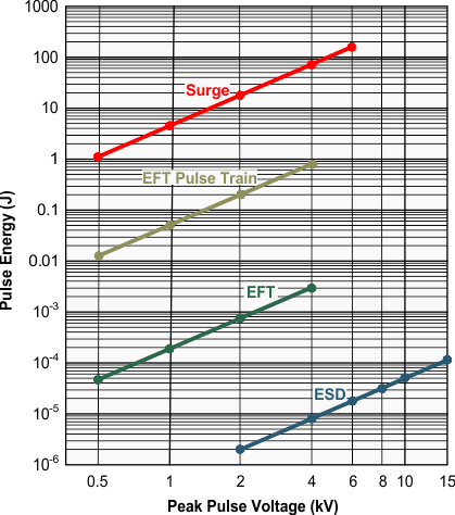
In the event of surge transients, high-energy content is characterized by long pulse duration and slow decaying pulse power. The electrical energy of a transient that is dumped into the internal protection cells of a transceiver is converted into thermal energy, which heats and destroys the protection cells, thus destroying the transceiver. Figure 9-5 shows the large differences in transient energies for single ESD, EFT, surge transients, and an EFT pulse train that is commonly applied during compliance testing.
 Figure 9-5 Comparison of Transient Energies