SLLSF79B April 2021 – September 2021 THVD1439 , THVD1439V , THVD1449 , THVD1449V
PRODUCTION DATA
- 1 Features
- 2 Applications
- 3 Description
- 4 Revision History
- 5 Pin Configuration and Functions
-
6 Specifications
- 6.1 Absolute Maximum Ratings
- 6.2 ESD Ratings
- 6.3 ESD Ratings, IEC
- 6.4 Recommended Operating Conditions
- 6.5 Thermal Information
- 6.6 Power Dissipation
- 6.7 Electrical Characteristics
- 6.8 Switching Characteristics (THVD1439, THVD1439V)
- 6.9 Switching Characteristics (THVD1449, THVD1449V)
- 6.10 Typical Characteristics
- 7 Parameter Measurement Information
- 8 Detailed Description
- 9 Application and Implementation
- 10Power Supply Recommendations
- 11Layout
- 12Device and Documentation Support
Package Options
Refer to the PDF data sheet for device specific package drawings
Mechanical Data (Package|Pins)
- D|8
Thermal pad, mechanical data (Package|Pins)
Orderable Information
3 Description
THVD14x9(V) devices are half-duplex RS-485 transceivers with integrated surge protection. Surge protection is achieved by integrating transient voltage suppressor (TVS) diodes in the standard 8-pin SOIC (D) package. This feature increases the reliability by providing better immunity to noise transients coupled to the data cable which eliminates the need for external protection components.
THVD1439 and THVD1449 operate from a single
3.3-V or 5-V supply. The THVD1439V and THVD1449V devices support an additional VIO supply to operate the IOs from as low as 1.65 V supply level. The devices in this family feature a wide common-mode voltage range making them suitable for multi-point applications over long cable runs.
| PART NUMBER | PACKAGE(1) | BODY SIZE (NOM) |
|---|---|---|
| THVD1439 THVD1439V THVD1449 THVD1449V | SOIC (8) | 4.90 mm × 3.91 mm |
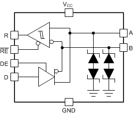
 THVD14x9 Block Diagram
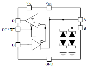
 THVD14x9V Block Diagram