SLLSF79B April 2021 – September 2021 THVD1439 , THVD1439V , THVD1449 , THVD1449V
PRODUCTION DATA
- 1 Features
- 2 Applications
- 3 Description
- 4 Revision History
- 5 Pin Configuration and Functions
-
6 Specifications
- 6.1 Absolute Maximum Ratings
- 6.2 ESD Ratings
- 6.3 ESD Ratings, IEC
- 6.4 Recommended Operating Conditions
- 6.5 Thermal Information
- 6.6 Power Dissipation
- 6.7 Electrical Characteristics
- 6.8 Switching Characteristics (THVD1439, THVD1439V)
- 6.9 Switching Characteristics (THVD1449, THVD1449V)
- 6.10 Typical Characteristics
- 7 Parameter Measurement Information
- 8 Detailed Description
- 9 Application and Implementation
- 10Power Supply Recommendations
- 11Layout
- 12Device and Documentation Support
Package Options
Refer to the PDF data sheet for device specific package drawings
Mechanical Data (Package|Pins)
- D|8
Thermal pad, mechanical data (Package|Pins)
Orderable Information
8.3.3 Surge Protection
Surge transients often result from lightning strikes (direct strike or an indirect strike which induce voltages and currents), or the switching of power systems, including load changes and short circuit switching. These transients are often encountered in industrial environments, such as factory automation and power-grid systems.
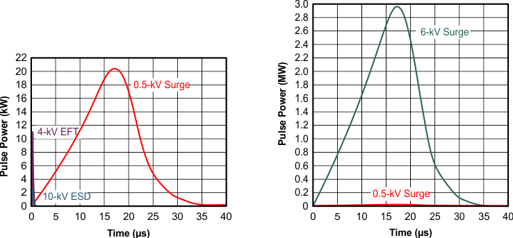
Figure 8-5 compares the pulse-power of the EFT and surge transients with the power caused by an IEC ESD transient. The diagram on the left shows the relative pulse-power for a 0.5-kV surge transient and 4-kV EFT transient, both of which dwarf the 10-kV ESD transient visible in the lower-left corner. 500-V surge transients are representative of events that may occur in factory environments in industrial and process automation.
The diagram on the right shows the pulse-power of a 6-kV surge transient, relative to the same 0.5-kV surge transient. 6-kV surge transients are most likely to occur in power generation and power-grid systems.
 Figure 8-5 Power Comparison of ESD, EFT, and Surge Transients
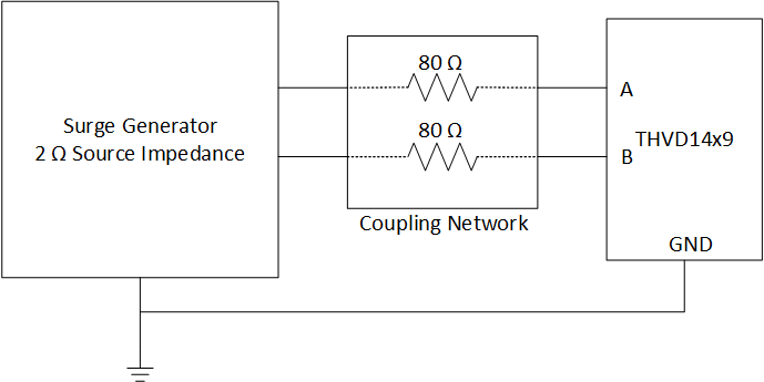
Figure 8-6 shows the test setup used to validate THVD14x9 surge performance according to the IEC 61000-4-5 1.2/50-μs surge pulse.
 Figure 8-6 THVD14x9(V) Surge Test Setup
THVD14x9(V) product family is robust to ±4-kV surge transients without the need for any external components. The transient current and voltage waveforms resulting from a +4-kV surge test as described in Figure 8-6 are shown in Figure 8-7. The bus pin voltage is clamped by the integrated surge protection diodes such that the internal circuitry is not damaged during the surge event. The clamping voltage at the bus pins for versus the total current from the surge generator is shown in Figure 8-8.