SCPS268A September   2017  – February 2022 TIC10024-Q1

PRODUCTION DATA  

  1. Features
  2. Applications
  3. Description
  4. Revision History
  5. Pin Configuration and Functions
  6. Specifications
    1. 6.1 Absolute Maximum Ratings
    2. 6.2 ESD Ratings
    3. 6.3 Recommended Operating Conditions
    4. 6.4 Thermal Information
    5. 6.5 Electrical Characteristics
    6. 6.6 Timing Requirements
    7. 6.7 Typical Characteristics
  7. Parameter Measurement Information
  8. Detailed Description
    1. 8.1 Overview
    2. 8.2 Functional Block Diagram
    3. 8.3 Feature Description
      1. 8.3.1  VS Pin
      2. 8.3.2  VDD Pin
      3. 8.3.3  Device Initialization
      4. 8.3.4  Device Trigger
      5. 8.3.5  Device Reset
        1. 8.3.5.1 VS Supply POR
        2. 8.3.5.2 Hardware Reset
        3. 8.3.5.3 Software Reset
      6. 8.3.6  VS Under-Voltage (UV) Condition
      7. 8.3.7  VS Over-Voltage (OV) Condition
      8. 8.3.8  Switch Inputs Settings
        1. 8.3.8.1 Input Current Source and Sink Selection
        2. 8.3.8.2 Input Enable Selection
        3. 8.3.8.3 Thresholds Adjustment
        4. 8.3.8.4 Wetting Current Configuration
      9. 8.3.9  Interrupt Generation and INT Assertion
        1. 8.3.9.1 INT Pin Assertion Scheme
        2. 8.3.9.2 Interrupt Idle Time (tINT_IDLE) Time
        3. 8.3.9.3 Microcontroller Wake-Up
        4. 8.3.9.4 Interrupt Enable / Disable And Interrupt Generation Conditions
        5. 8.3.9.5 Detection Filter
      10. 8.3.10 Temperature Monitor
        1. 8.3.10.1 Temperature Warning (TW)
        2. 8.3.10.2 Temperature Shutdown (TSD)
      11. 8.3.11 Parity Check And Parity Generation
      12. 8.3.12 Cyclic Redundancy Check (CRC)
    4. 8.4 Device Functional Modes
      1. 8.4.1 Continuous Mode
      2. 8.4.2 Polling Mode
      3. 8.4.3 Additional Features
        1. 8.4.3.1 Clean Current Polling (CCP)
        2. 8.4.3.2 Wetting Current Auto-Scaling
  9. Programming
    1. 9.1 SPI Communication Interface Buses
      1. 9.1.1 Chip Select ( CS)
      2. 9.1.2 System Clock (SCLK)
      3. 9.1.3 Slave In (SI)
      4. 9.1.4 Slave Out (SO)
    2. 9.2 SPI Sequence
      1. 9.2.1 Read Operation
      2. 9.2.2 Write Operation
      3. 9.2.3 Status Flag
    3. 9.3 Programming Guidelines
    4. 9.4 Register Maps
  10. 10Application and Implementation
    1. 10.1 Application Information
    2. 10.2 Digital Switch Detection in Automotive Body Control Module
      1. 10.2.1 Design Requirements
      2. 10.2.2 Detailed Design Procedure
      3. 10.2.3 Application Curves
    3. 10.3 Systems Examples
      1. 10.3.1 Using TIC10024-Q1 in a 12 V Automotive System
  11. 11Power Supply Recommendations
  12. 12Layout
    1. 12.1 Layout Guidelines
    2. 12.2 Layout Example
  13. 13Device and Documentation Support
    1. 13.1 Receiving Notification of Documentation Updates
    2. 13.2 Community Resources
    3. 13.3 Trademarks
  14. 14Mechanical, Packaging, and Orderable Information

Package Options

Mechanical Data (Package|Pins)
Thermal pad, mechanical data (Package|Pins)
Orderable Information

Digital Switch Detection in Automotive Body Control Module

The body control module (BCM) is an electronic control unit responsible for monitoring and controlling various electronic accessories in a vehicle body. Detection of various mechanical switches status in a vehicle is one important task handled by the BCM. Most switches inside the BCM are digital in nature, meaning they have either an ON or an OFF state. The TIC10024-Q1 can detect up to 24 digital switches. The following application diagram depicts how the TIC10024-Q1 is used in a BCM to detect an external digital switch and a detailed design example is shown in the following sections.
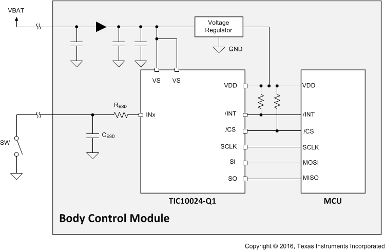
GUID-2FE25055-AA32-45DD-AA78-7DA40DDB8203-low.gifFigure 10-1 Using TIC10024-Q1 to Monitor a Digital Switch in Body Control Module Application