SLLSFJ1D February 2022 – March 2023 TIOL112 , TIOL1123 , TIOL1125
PRODUCTION DATA
- 1 Features
- 2 Applications
- 3 Description
- 4 Revision History
- 5 Pin Configuration and Functions
- 6 Specifications
- 7 Parameter Measurement Information
-
8 Detailed Description
- 8.1 Overview
- 8.2 Functional Block Diagrams
- 8.3
Feature Description
- 8.3.1 Wake-Up Detection
- 8.3.2 Current Limit Configuration
- 8.3.3 Current Fault Detection, Indication and Auto Recovery
- 8.3.4 Thermal Warning, Thermal Shutdown
- 8.3.5 Fault Reporting (NFAULT)
- 8.3.6 Transceiver Function Tables
- 8.3.7 The Integrated Voltage Regulator (LDO)
- 8.3.8 Reverse Polarity Protection
- 8.3.9 Integrated Surge Protection and Transient Waveform Tolerance
- 8.3.10 Power Up Sequence (TIOL112)
- 8.3.11 Undervoltage Lock-Out (UVLO)
- 8.4 Device Functional Modes
- 9 Application and Implementation
- 10Device and Documentation Support
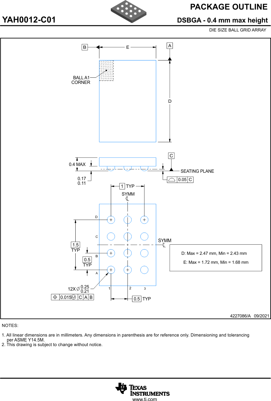
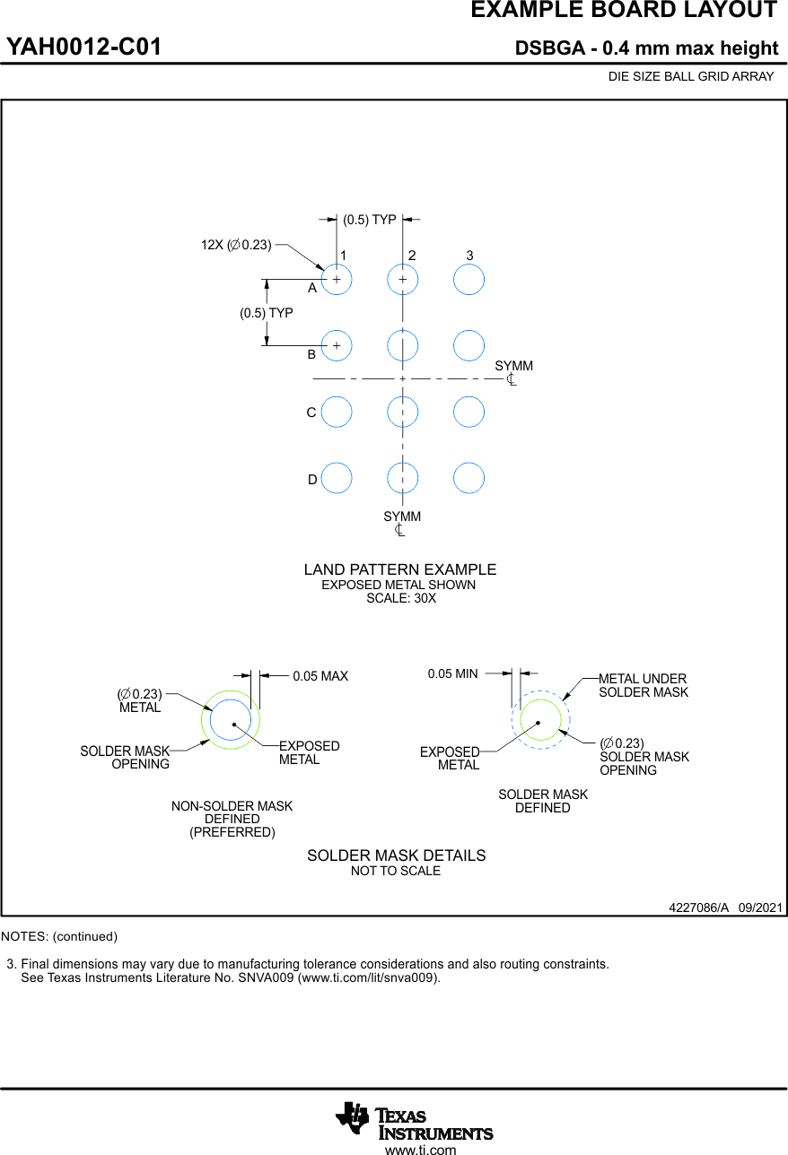
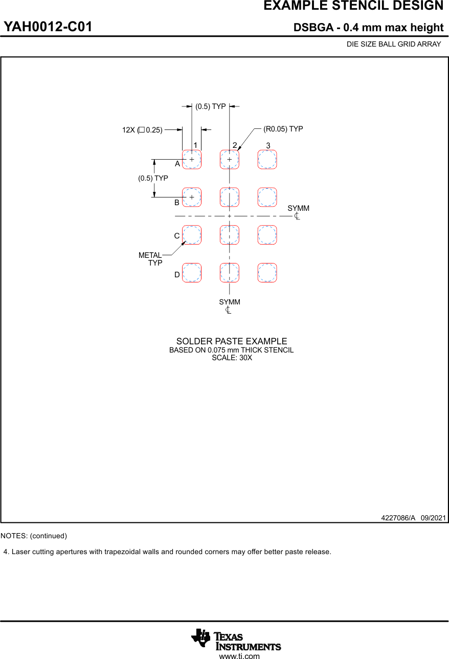
- 11Mechanical, Packaging, and Orderable Information
Package Options
Mechanical Data (Package|Pins)
- YAH|12
- DRC|10
Thermal pad, mechanical data (Package|Pins)
- DRC|10
Orderable Information
11 Mechanical, Packaging, and Orderable Information
The following pages include mechanical, packaging, and orderable information. This information is the most current data available for the designated devices. This data is subject to change without notice and revision of this document. For browser-based versions of this data sheet, refer to the left-hand navigation.