SLOS081M February 1977 – December 2021 TL081 , TL081A , TL081B , TL081H , TL082 , TL082A , TL082B , TL082H , TL084 , TL084A , TL084B , TL084H
PRODUCTION DATA
- 1 Features
- 2 Applications
- 3 Description
- 4 Revision History
- 5 Pin Configuration and Functions
-
6 Specifications
- 6.1 Absolute Maximum Ratings: TL08xH
- 6.2 Absolute Maximum Ratings: All Other Devices
- 6.3 ESD Ratings: TL08xH
- 6.4 ESD Ratings: All Other Devices
- 6.5 Recommended Operating Conditions: TL08xH
- 6.6 Recommended Operating Conditions: All Other Devices
- 6.7 Thermal Information for Single Channel: TL081H
- 6.8 Thermal Information for Dual Channel: TL082H
- 6.9 Thermal Information for Quad Channel: TL084H
- 6.10 Thermal Information: All Other Devices
- 6.11 Electrical Characteristics: TL08xH
- 6.12 Electrical Characteristics for TL08xC, TL08xxC, and TL08xI
- 6.13 Electrical Characteristics for TL08xM and TL084x
- 6.14 Switching Characteristics
- 6.15 Dissipation Rating Table
- 6.16 Typical Characteristics: TL08xH
- 6.17 Typical Characteristics: All Other Devices
- 7 Parameter Measurement Information
- 8 Detailed Description
- 9 Applications and Implementation
- 10Power Supply Recommendations
- 11Layout
- 12Device and Documentation Support
- 13Mechanical, Packaging, and Orderable Information
Package Options
Refer to the PDF data sheet for device specific package drawings
Mechanical Data (Package|Pins)
- D|8
- P|8
Thermal pad, mechanical data (Package|Pins)
- D|8
Orderable Information
6.17 Typical Characteristics: All Other Devices
Data at high and low temperatures are applicable only within the rated operating free-air temperature ranges of the various devices. The Figure numbers referenced in the following graphs are located in Section 7.
 Figure 6-40 Maximum Peak Output Voltage vs Frequency
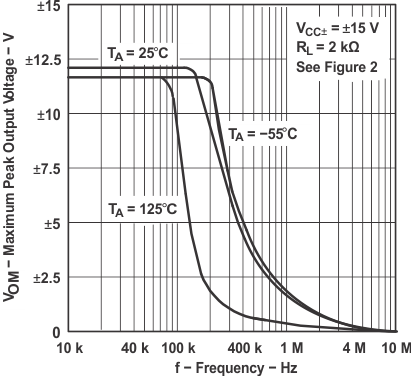 Figure 6-42 Maximum Peak Output Voltage vs Frequency
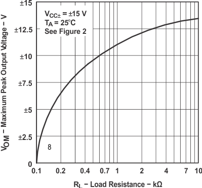 Figure 6-44 Maximum Peak Output Voltage vs Load Resistance
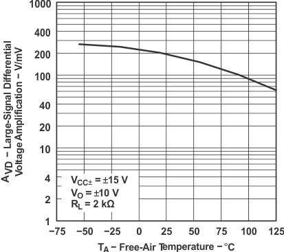 Figure 6-46 Large-Signal Differential Voltage Amplification vs Free-Air Temperature
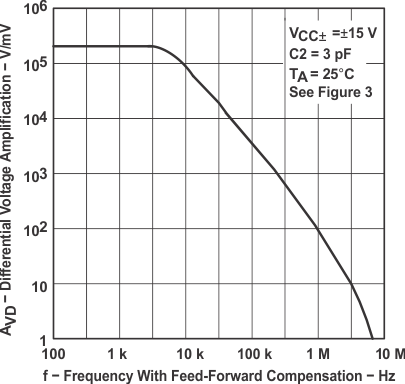 Figure 6-48 Differential Voltage Amplification vs Frequency with Feed-Forward Compensation
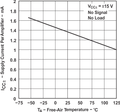 Figure 6-50 Supply Current per Amplifier vs Free-Air Temperature
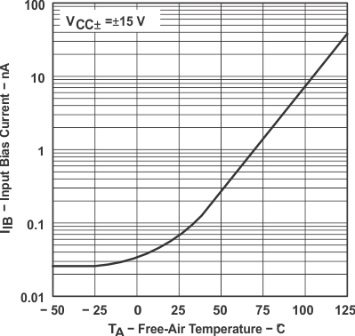 Figure 6-52 Input Bias Current vs Free-Air Temperature
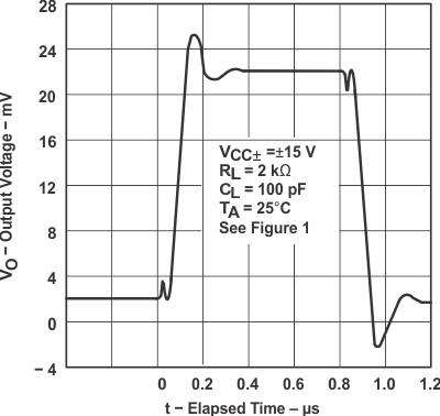 Figure 6-54 Output Voltage vs Elapsed Time
 Figure 6-56 Equivalent Input Noise Voltage vs Frequency
 Figure 6-41 Maximum Peak Output Voltage vs Frequency
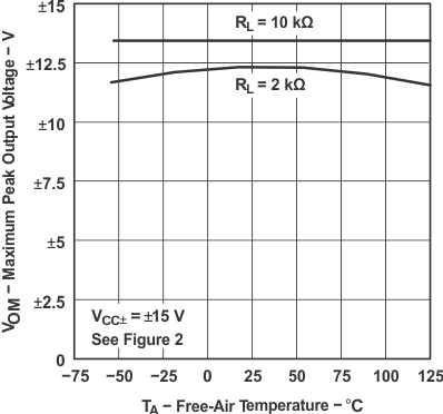 Figure 6-43 Maximum Peak Output Voltage vs Free-Air Temperature
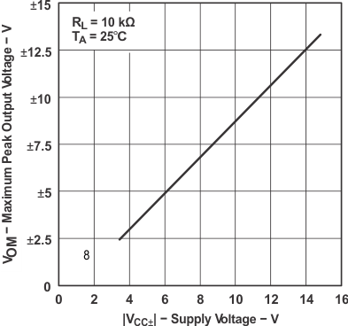 Figure 6-45 Maximum Peak Output Voltage vs Supply Voltage
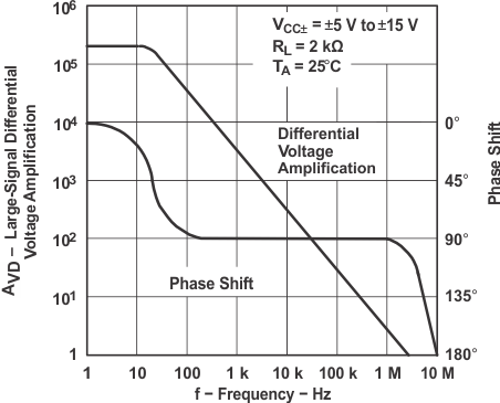 Figure 6-47 Large-Signal Differential Voltage Amplification and Phase Shift vs Frequency
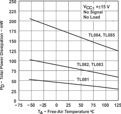 Figure 6-49 Total Power Dissipation vs Free-Air Temperature
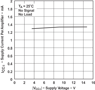 Figure 6-51 Supply Current per Amplifier vs Supply Voltage
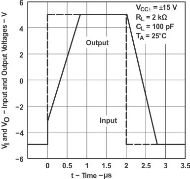 Figure 6-53 Voltage-Follower Large-Signal Pulse Response
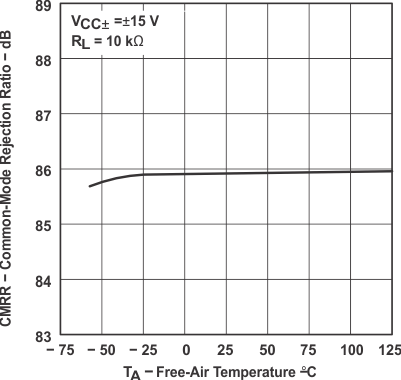 Figure 6-55 Common-Mode Rejection Ratio vs Free-Air Temperature
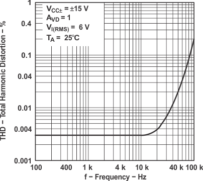 Figure 6-57 Total Harmonic Distortion vs Frequency