SLLS177I March 1994 – March 2021 TL16C550C
PRODUCTION DATA
- 1 Features
- 2 Description
- 3 Revision History
- 4 Pin Configuration and Functions
-
5 Specifications
- 5.1 Absolute Maximum Ratings
- 5.2 Recommended Operating Conditions (Low Voltage - 3.3 nominal)
- 5.3 Recommended Operating Conditions (Standard Voltage - 5 V nominal)
- 5.4 Thermal Information
- 5.5 Electrical Characteristics (Low Voltage - 3.3 V nominal)
- 5.6 Electrical Characteristics (Standard Voltage - 5 V nominal)
- 5.7 System Timing Requirements
- 5.8 System Switching Characteristics
- 5.9 Baud Generator Switching Characteristics
- 5.10 Receiver Switching Characteristics
- 5.11 Transmitter Switching Characteristics
- 5.12 Modem Control Switching Characteristics
- 6 Parameter Measurement Information
-
7 Detailed Description
- 7.1 Autoflow Control (see Figure 1-1)
- 7.2 Auto-RTS (see Figure 1-1)
- 7.3 Auto-CTS (see Figure 1-1)
- 7.4 Enabling Autoflow Control and Auto-CTS
- 7.5 Auto-CTS and Auto-RTS Functional Timing
- 7.6 Functional Block Diagram
- 7.7
Principles of Operation
- 7.7.1 Accessible Registers
- 7.7.2 FIFO Control Register (FCR)
- 7.7.3 FIFO Interrupt Mode Operation
- 7.7.4 FIFO Polled Mode Operation
- 7.7.5 Interrupt Enable Register (IER)
- 7.7.6 Interrupt Identification Register (IIR)
- 7.7.7 Line Control Register (LCR)
- 7.7.8 Line Status Register (LSR)
- 7.7.9 Modem Control Register (MCR)
- 7.7.10 Modem Status Register (MSR)
- 7.7.11 Programming Baud Generator
- 7.7.12 Receiver Buffet Register (RBR)
- 7.7.13 Scratch Register
- 7.7.14 Transmitter Holding Register (THR)
- 8 Application Information
- 9 Device and Documentation Support
- 10Mechanical, Packaging, and Orderable Information
Package Options
Mechanical Data (Package|Pins)
Thermal pad, mechanical data (Package|Pins)
- PFB|48
Orderable Information
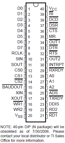
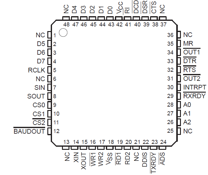
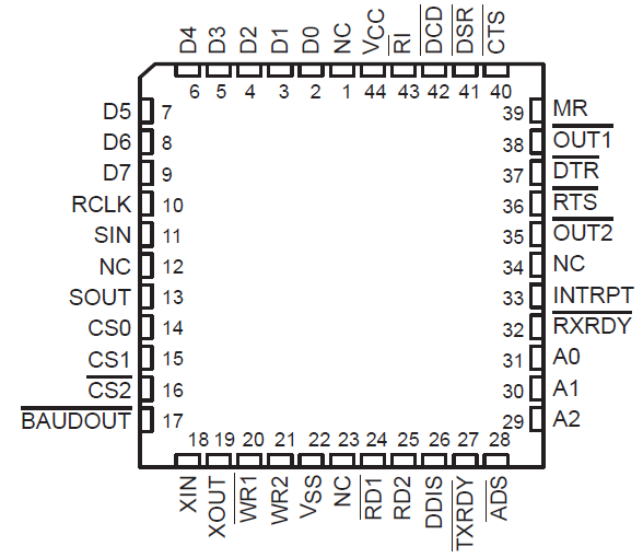
4 Pin Configuration and Functions
 Figure 4-1 N Package (Top View)
 Figure 4-3 PT/PFB Package (Top View)
 Figure 4-2 FN Package (Top View)
NC - No internal connection
Table 4-1 Pin Functions
| TERMINAL | I/O | DESCRIPTION | |||
|---|---|---|---|---|---|
| NAME | NO.N(1) | NO.FN | NO.PT | ||
| A0 | 28 | 31 | 28 | I | Register select. A0 −A2 are used during read and write operations to select the ACE register to read from or write to. Refer to Table 1 for register addresses and refer to ADS description. |
| A1 | 27 | 30 | 27 | ||
| A2 | 26 | 29 | 26 | ||
| ADS | 25 | 28 | 24 | I | Address strobe. When ADS is active (low), A0, A1, and A2 and CS0, CS1, and CS2 drive the internal select logic directly; when ADS is high, the register select and chip select signals are held at the logic levels they were in when the low-to-high transition of ADS occurred |
| BAUDOUT | 15 | 17 | 12 | O | Baud out. BAUDOUT is a 16 x clock signal for the transmitter section of the ACE. The clock rate is established by the reference oscillator frequency divided by a divisor specified by the baud generator divisor latches. BAUDOUT may also be used for the receiver section by tying this output to RCLK. |
| CS0 | 12 | 14 | 9 | I | Chip select. When CS0 and CS1 are high and CS2 is low, these three inputs select the ACE. When any of these inputs are inactive, the ACE remains inactive (refer to ADS description). |
| CS1 | 13 | 15 | 10 | ||
| CS2 | 14 | 16 | 11 | ||
| CTS | 36 | 40 | 38 | I | Clear to send. CTS is a modem status signal. Its condition can be checked by reading bit 4 (CTS) of the modem status register. Bit 0 (ΔCTS) of the modem status register indicates that CTS has changed states since the last read from the modem status register. If the modem status interrupt is enabled when CTS changes levels and the auto-CTS mode is not enabled, an interrupt is generated. CTS is also used in the auto-CTS mode to control the transmitter |
| D0 | 1 | 2 | 43 | I/O | Data bus. Eight data lines with 3-state outputs provide a bidirectional path for data, control, and status information between the ACE and the CPU. |
| D1 | 2 | 3 | 44 | ||
| D2 | 3 | 4 | 45 | ||
| D3 | 4 | 5 | 46 | ||
| D4 | 5 | 6 | 47 | ||
| D5 | 6 | 7 | 2 | ||
| D6 | 7 | 8 | 3 | ||
| D7 | 8 | 9 | 4 | ||
| DCD | 38 | 42 | 40 | I | Data carrier detect. DCD is a modem status signal. Its condition can be checked by reading bit 7 (DCD) of the modem status register. Bit 3 (ΔDCD) of the modem status register indicates that DCD has changed states since the last read from the modem status register. If the modem status interrupt is enabled when DCD changes levels, an interrupt is generated |
| DDIS | 23 | 26 | 22 | O | Driver disable. DDIS is active (high) when the CPU is not reading data. When active, DDIS can disable an external transceiver. |
| DSR | 37 | 41 | 39 | I | Data set ready. DSR is a modem status signal. Its condition can be checked by reading bit 5 (DSR) of the modem status register. Bit 1 (ΔDSR) of the modem status register indicates DSR has changed levels since the last read from the modem status register. If the modem status interrupt is enabled when DSR changes levels, an interrupt is generated. |
| DTR | 33 | 37 | 33 | O | Data terminal ready. When active (low), DTR informs a modem or data set that the ACE is ready to establish comunication. DTR is placed in the active level by setting the DTR bit of the modem control register. DTR is placed in the inactive level either as a result of a master reset, during loop mode operation, or clearing the DTR bit. |
| INTRPT | 30 | 33 | 30 | O | Interrupt.When active (high), INTRPT informs the CPU that the ACE has an interrupt to be serviced. Four conditions that cause an interrupt to be issued are: a receiver error, received data that is available or timed out (FIFO mode only), an empty transmitter holding register, or an enabled modem status interrupt. INTRPT is reset (deactivated) either when the interrupt is serviced or as a result of a master reset. |
| MR | 35 | 39 | 35 | I | Master reset. When active (high), MR clears most ACE registers and sets the levels of various output signals (refer to Table 2). |
| OUT1 | 34 | 38 | 34 | O | Outputs 1 and 2. These are user-designated output terminals that are set to the active (low) level by setting respective modem control register (MCR) bits (OUT1 and OUT2). OUT1 and OUT2 are set to inactive the (high) level as a result of master reset, during loop mode operations, or by clearing bit 2 (OUT1) or bit 3 (OUT2) of the MCR. |
| OUT2 | 31 | 35 | 31 | ||
| RCLK | 9 | 10 | 5 | I | Receiver clock. RCLK is the 16 x baud rate clock for the receiver section of the ACE. |
| RD1 | 21 | 24 | 19 | I | Read inputs. When either RD1 or RD2 is active (low or high respectively) while the ACE is selected, the CPU is allowed to read status information or data from a selected ACE register. Only one of these inputs is required for the transfer of data during a read operation; the other input should be tied to its inactive level (i.e., RD2 tied low or RD1 tied high |
| RD2 | 22 | 25 | 20 | ||
| RI | 39 | 43 | 41 | I | Ring indicator. RI is a modem status signal. Its condition can be checked by reading bit 6 (RI) of the modem status register. Bit 2 (TERI) of the modem status register indicates that RI has transitioned from a low to a high level since the last read from the modem status register. If the modem status interrupt is enabled when this transition occurs, an interrupt is generated |
| RTS | 32 | 36 | 32 | O | Request to send. When active, RTS informs the modem or data set that the ACE is ready to receive data. RTS is set to the active level by setting the RTS modem control register bit and is set to the inactive (high) level either as a result of a master reset or during loop mode operations or by clearing bit 1 (RTS) ofthe MCR. In the auto-RTS mode, RTS is set to the inactive level by the receiver threshold control logic |
| RXRDY | 29 | 32 | 29 | O | Receiver ready. Receiver direct memory access (DMA) signalling is available with RXRDY. When operating in the FIFO mode, one of two types of DMA signalling can be selected using the FIFO control register bit 3 (FCR3). When operating in the TL16C450 mode, only DMA mode 0 is allowed. Mode 0 supports single-transfer DMA in which a transfer is made between CPU bus cycles. Mode 1 supports multitransfer DMA in which multiple transfers are made continuously until the receiver FIFO has been emptied. In DMA mode 0 (FCR0 = 0 or FCR0 =1, FCR3 = 0), when there is at least one character in the receiver FIFO or receiver holding register, RXRDY is active (low). When RXRDY has been active but there are no characters in the FIFO or holding register, RXRDY goes inactive (high).In DMA mode 1 (FCR0 = 1, FCR3 = 1), when the trigger level or the time-out has been reached, RXRDY goes active (low); when it has been active but there are no more characters in the FIFO or holding register, it goes inactive (high). |
| SIN | 10 | 11 | 7 | I | Serial data input. SIN is serial data input from a connected communications device. |
| SOUT | 11 | 13 | 8 | O | Serial data output. SOUT is composite serial data output to a connected communication device. SOUT is set to the marking (high) level as a result of master reset. |
| TXRDY | 24 | 27 | 23 | O | Transmitter ready. Transmitter DMA signalling is available with TXRDY. When operating in the FIFO mode, one of two types of DMA signalling can be selected using FCR3. When operating in the TL16C450 mode, only DMA mode 0 is allowed. Mode 0 supports single-transfer DMA in which a transfer is made between CPU bus cycles. Mode 1 supports multitransfer DMA in which multiple transfers are made continuously until the transmit FIFO has been filled. |
| VCC | 40 | 44 | 42 | 5-V supply voltage | |
| VSS | 20 | 22 | 18 | Supply common | |
| WR1 | 18 | 20 | 16 | I | Write inputs. When either WR1 or WR2 is active (low or high respectively) and while the ACE is selected,the CPU is allowed to write control words or data into a selected ACE register. Only one of these inputs is required to transfer data during a write operation; the other input should be tied to its inactive level (i.e., WR2 tied low or WR1 tied high). |
| WR2 | 19 | 21 | 17 | ||
| XIN | 16 | 18 | 14 | I/O | External clock. XIN and XOUT connect the ACE to the main timing reference (clock or crystal). |
| XOUT | 17 | 19 | 15 | ||
(1) The N package is Not Recommended for
New Designs.