SNVSBA4A May 2019 – November 2019 TL431LI-Q1 , TL432LI-Q1
PRODUCTION DATA.
- 1 Features
- 2 Applications
- 3 Description
- 4 Revision History
- 5 Device Comparison Table
- 6 Pin Configuration and Functions
- 7 Specifications
- 8 Parameter Measurement Information
- 9 Detailed Description
-
10Applications and Implementation
- 10.1 Application Information
- 10.2 Typical Applications
- 10.3 System Examples
- 11Power Supply Recommendations
- 12Layout
- 13Device and Documentation Support
- 14Mechanical, Packaging, and Orderable Information
Package Options
Mechanical Data (Package|Pins)
- DBZ|3
Thermal pad, mechanical data (Package|Pins)
Orderable Information
7.6 Typical Characteristics
Data at high and low temperatures are applicable only within the recommended operating free-air temperature ranges of the various devices.
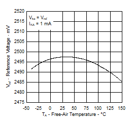 Figure 1. Reference Voltage versus Free-Air Temperature
 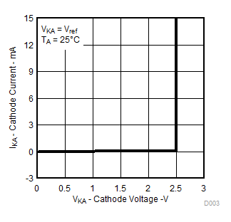 Figure 3. Cathode Current versus Cathode Voltage
 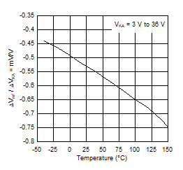 Figure 5. Ratio of Delta Reference Voltage to Delta Cathode Voltage versus Free-Air Temperature
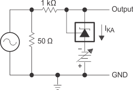
 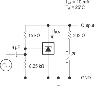 Figure 7. Test Circuit for Voltage Amplification
1.
Figure 9. Test Circuit for Reference Impedance 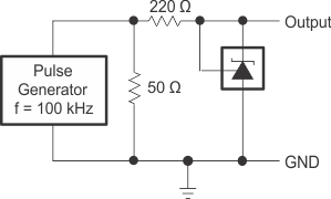
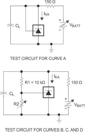 Figure 13. Test Circuits for Stability Boundary Conditions
 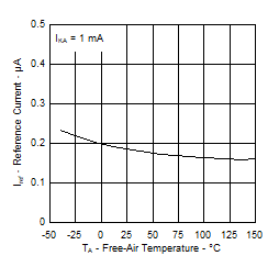 Figure 2. Reference Current versus Free-Air Temperature
 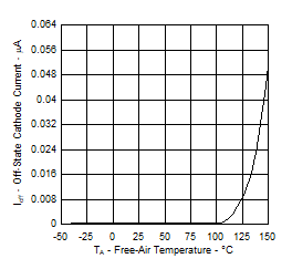 Figure 4. Off-State Cathode Current
versus Free-Air Temperature
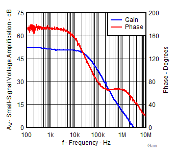 Figure 6. Small-Signal Voltage Amplification
versus Frequency
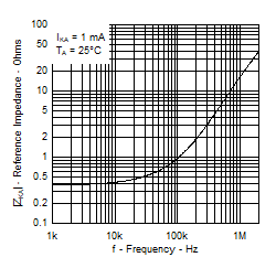 Figure 8. Reference Impedance versus Frequency
 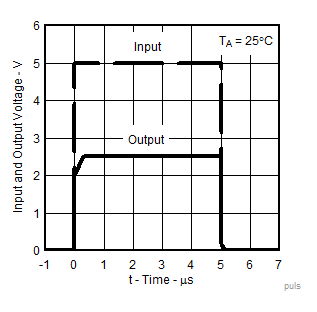 Figure 10. Pulse Response
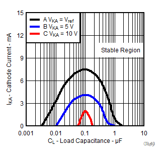
A. The areas under the curves represent conditions that may cause the device to oscillate. For curves B and C, R2 and V+ are adjusted to establish the initial VKA and IKA conditions, with CL = 0. VBATT and CL then are adjusted to determine the ranges of stability.
Figure 12. Stability Boundary Conditions for All TL431LI-Q1, TL432LI-Q1 Devices