SLVS074I January 1983 – July 2022 TL494
PRODUCTION DATA
- 1 Features
- 2 Applications
- 3 Description
- 4 Simplified Block Diagram
- 5 Revision History
- 6 Pin Configuration and Functions
-
7 Specifications
- 7.1 Absolute Maximum Ratings
- 7.2 ESD Ratings
- 7.3 Recommended Operating Conditions
- 7.4 Thermal Information
- 7.5 Electrical Characteristics, Reference Section
- 7.6 Electrical Characteristics, Oscillator Section
- 7.7 Electrical Characteristics, Error-Amplifier Section
- 7.8 Electrical Characteristics, Output Section
- 7.9 Electrical Characteristics, Dead-Time Control Section
- 7.10 Electrical Characteristics, PWM Comparator Section
- 7.11 Electrical Characteristics, Total Device
- 7.12 Switching Characteristics
- 7.13 Typical Characteristics
- 8 Parameter Measurement Information
- 9 Detailed Description
- 10Application and Implementation
- 11Power Supply Recommendations
- 12Layout
- 13Device and Documentation Support
- 14Mechanical, Packaging, and Orderable Information
Package Options
Mechanical Data (Package|Pins)
Thermal pad, mechanical data (Package|Pins)
Orderable Information
10.2.2.2.4 Soft Start and Dead Time
To reduce stress on the switching transistors at the start-up time, the start-up surge that occurs as the output filter capacitor charges must be reduced. The availability of the dead-time control makes implementation of a soft-start circuit relatively simple (see Figure 10-5).
 Figure 10-5 Soft-Start Circuit
The soft-start circuit allows the pulse width at the output to increase slowly (see Figure 10-5) by applying a negative slope waveform to the dead-time control input (pin 4).
Initially, capacitor C2 forces the dead-time control input to follow the 5-V regulator, which disables the outputs (100% dead time). As the capacitor charges through R6, the output pulse width slowly increases until the control loop takes command. With a resistor ratio of 1:10 for R6 and R7, the voltage at pin 4 after start-up is 0.1 × 5 V, or 0.5 V.
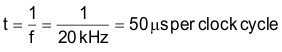
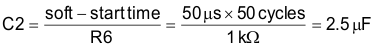
The soft-start time generally is in the range of 25 to 100 clock cycles. If 50 clock cycles at a 20-kHz switching rate is selected, the soft-start time is:
The value of the capacitor then is determined by:
This helps eliminate any false signals that might be created by the control circuit as power is applied.