SLVS074I January 1983 – July 2022 TL494
PRODUCTION DATA
- 1 Features
- 2 Applications
- 3 Description
- 4 Simplified Block Diagram
- 5 Revision History
- 6 Pin Configuration and Functions
-
7 Specifications
- 7.1 Absolute Maximum Ratings
- 7.2 ESD Ratings
- 7.3 Recommended Operating Conditions
- 7.4 Thermal Information
- 7.5 Electrical Characteristics, Reference Section
- 7.6 Electrical Characteristics, Oscillator Section
- 7.7 Electrical Characteristics, Error-Amplifier Section
- 7.8 Electrical Characteristics, Output Section
- 7.9 Electrical Characteristics, Dead-Time Control Section
- 7.10 Electrical Characteristics, PWM Comparator Section
- 7.11 Electrical Characteristics, Total Device
- 7.12 Switching Characteristics
- 7.13 Typical Characteristics
- 8 Parameter Measurement Information
- 9 Detailed Description
- 10Application and Implementation
- 11Power Supply Recommendations
- 12Layout
- 13Device and Documentation Support
- 14Mechanical, Packaging, and Orderable Information
Package Options
Mechanical Data (Package|Pins)
Thermal pad, mechanical data (Package|Pins)
Orderable Information
10.2.2.2.3 Current-Limiting Amplifier
The power supply was designed for a 10-A load current and an IL swing of 1.5 A, therefore, the short-circuit current should be:
Equation 10. 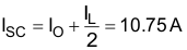
The current-limiting circuit is shown in Figure 10-4.
 Figure 10-4 Current-Limiting Circuit
Resistors R1 and R2 set the reference of approximately 1 V on the inverting input of the current-limiting amplifier. Resistor R13, in series with the load, applies 1 V to the non-inverting terminal of the current-limiting amplifier when the load current reaches 10 A. The output pulse width reduces accordingly. The value of R13 is calculated in Equation 11.
Equation 11. 