SLVS074I January 1983 – July 2022 TL494
PRODUCTION DATA
- 1 Features
- 2 Applications
- 3 Description
- 4 Simplified Block Diagram
- 5 Revision History
- 6 Pin Configuration and Functions
-
7 Specifications
- 7.1 Absolute Maximum Ratings
- 7.2 ESD Ratings
- 7.3 Recommended Operating Conditions
- 7.4 Thermal Information
- 7.5 Electrical Characteristics, Reference Section
- 7.6 Electrical Characteristics, Oscillator Section
- 7.7 Electrical Characteristics, Error-Amplifier Section
- 7.8 Electrical Characteristics, Output Section
- 7.9 Electrical Characteristics, Dead-Time Control Section
- 7.10 Electrical Characteristics, PWM Comparator Section
- 7.11 Electrical Characteristics, Total Device
- 7.12 Switching Characteristics
- 7.13 Typical Characteristics
- 8 Parameter Measurement Information
- 9 Detailed Description
- 10Application and Implementation
- 11Power Supply Recommendations
- 12Layout
- 13Device and Documentation Support
- 14Mechanical, Packaging, and Orderable Information
Package Options
Mechanical Data (Package|Pins)
Thermal pad, mechanical data (Package|Pins)
Orderable Information
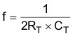
9.3.2 Oscillator
The oscillator provides a positive sawtooth waveform to the dead-time and PWM comparators for comparison to the various control signals.
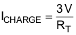
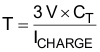
The frequency of the oscillator is programmed by selecting timing components RT and CT. The oscillator charges the external timing capacitor, CT, with a constant current, the value of which is determined by the external timing resistor, RT. This produces a linear-ramp voltage waveform. When the voltage across CT reaches 3 V, the oscillator circuit discharges it, and the charging cycle is reinitiated. The charging current is determined by the formula:
The period of the sawtooth waveform is:
The frequency of the oscillator becomes:
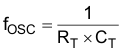
However, the oscillator frequency is equal to the output frequency only for single-ended applications. For push-pull applications, the output frequency is one-half the oscillator frequency.
Single-ended applications:

Push-pull applications: