SLVS037O September 1989 – December 2020 TL7702B , TL7705B , TL7733B
PRODUCTION DATA
- 1 Features
- 2 Applications
- 3 Description
- 4 Revision History
- 5 Pin Configuration and Functions
- 6 Specifications
- 7 Parameter Measurement Information
- 8 Detailed Description
- 9 Application and Implementation
- 10Power Supply Recommendations
- 11Layout
- 12Device and Documentation Support
- 13Mechanical, Packaging, and Orderable Information
Package Options
Refer to the PDF data sheet for device specific package drawings
Mechanical Data (Package|Pins)
- D|8
- P|8
Thermal pad, mechanical data (Package|Pins)
Orderable Information
8.4 Device Functional Modes
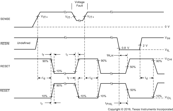
Figure 8-1 displays how the RESET and RESET output pins respond to the change in the the SENSE and RESIN input pins. When the RESIN pin is high, the RESET outputs are able to respond to a drop in the supply voltage at the SENSE pin. When the RESIN pin is low, the RESET and RESET pins are set HIGH and LOW respectively.
 Figure 8-1 TL77xxB RESET and
RESET Response and Timing